Portfolio Highlights
Cubic Awe
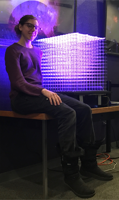
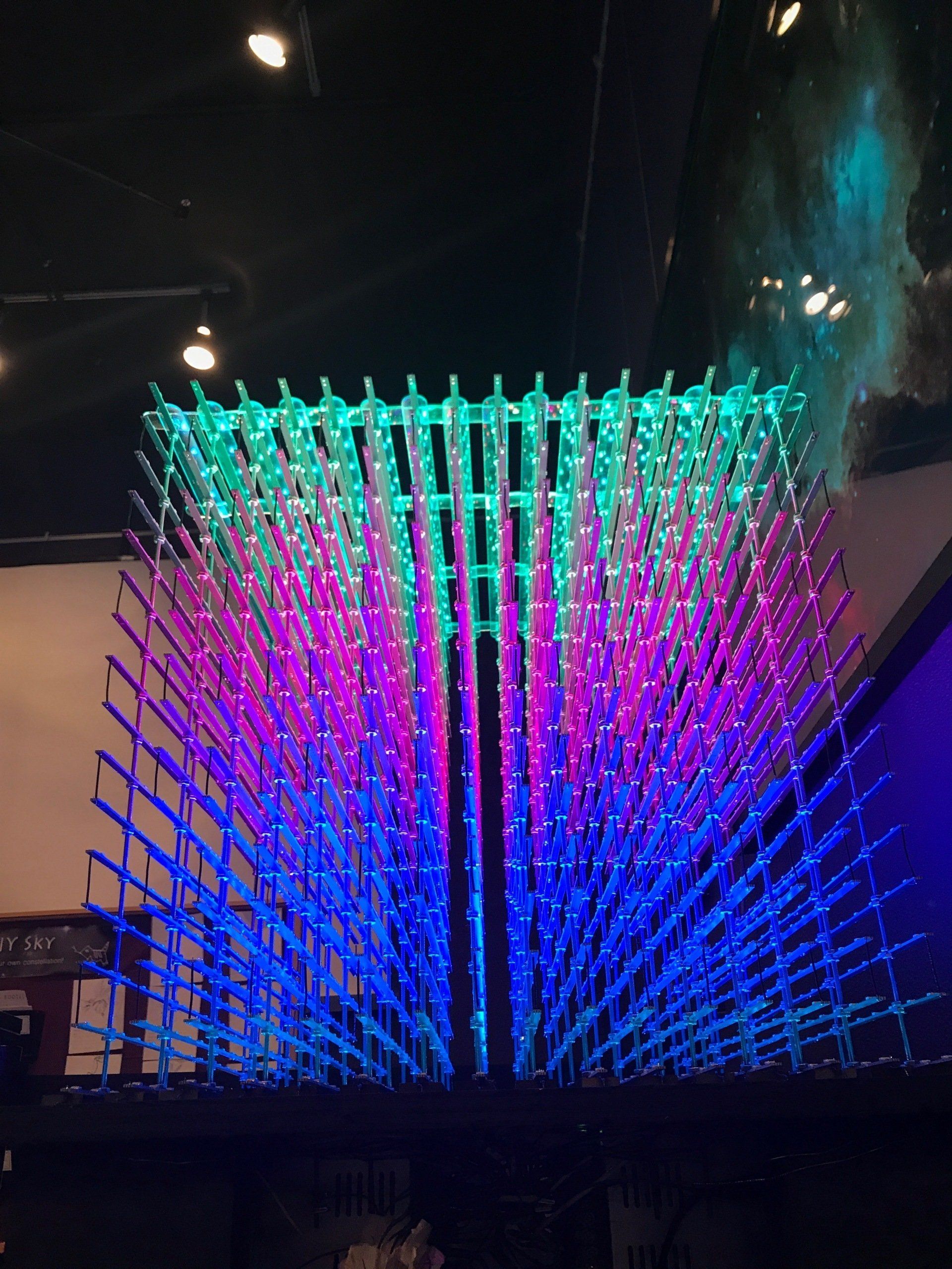
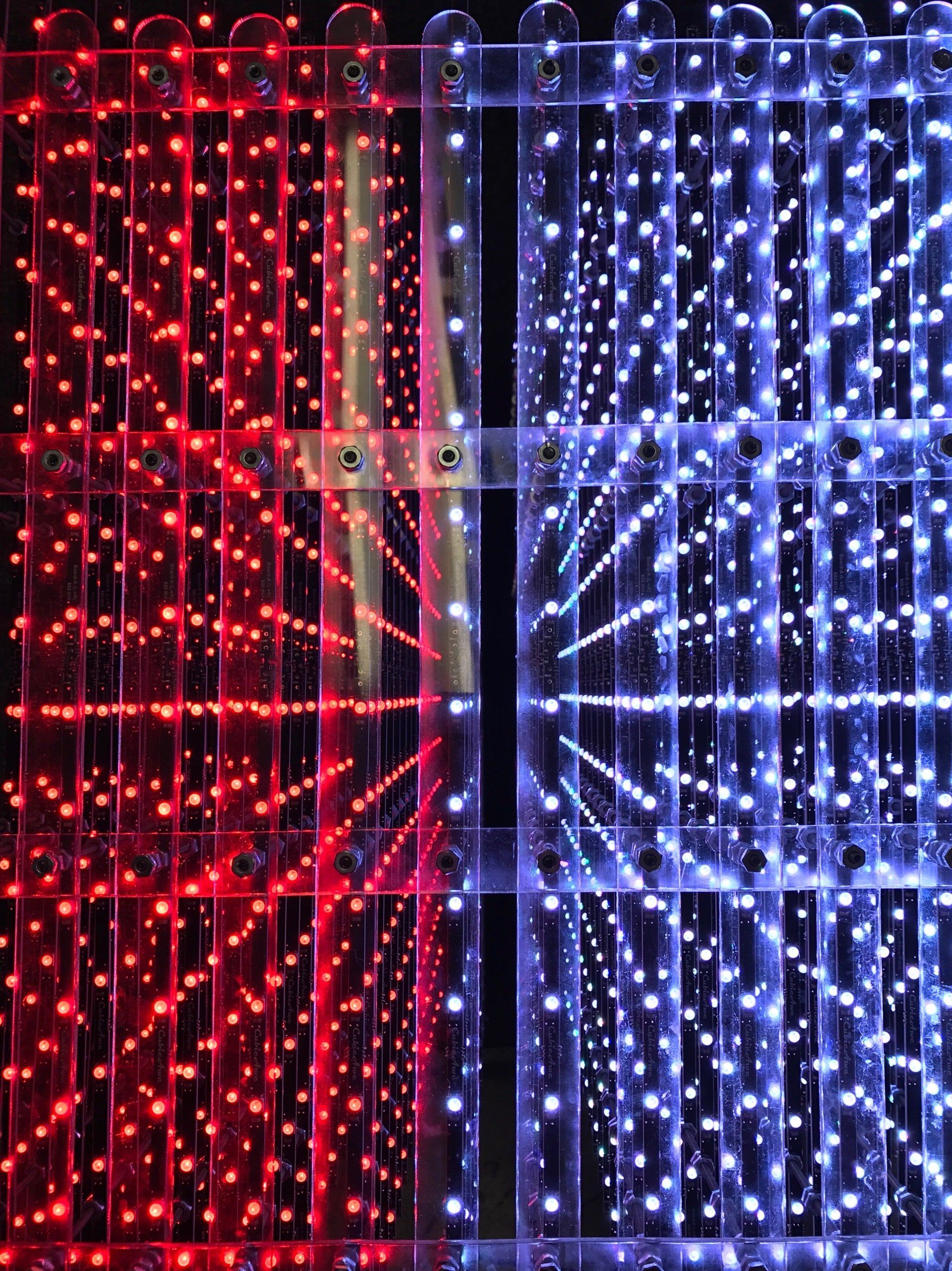
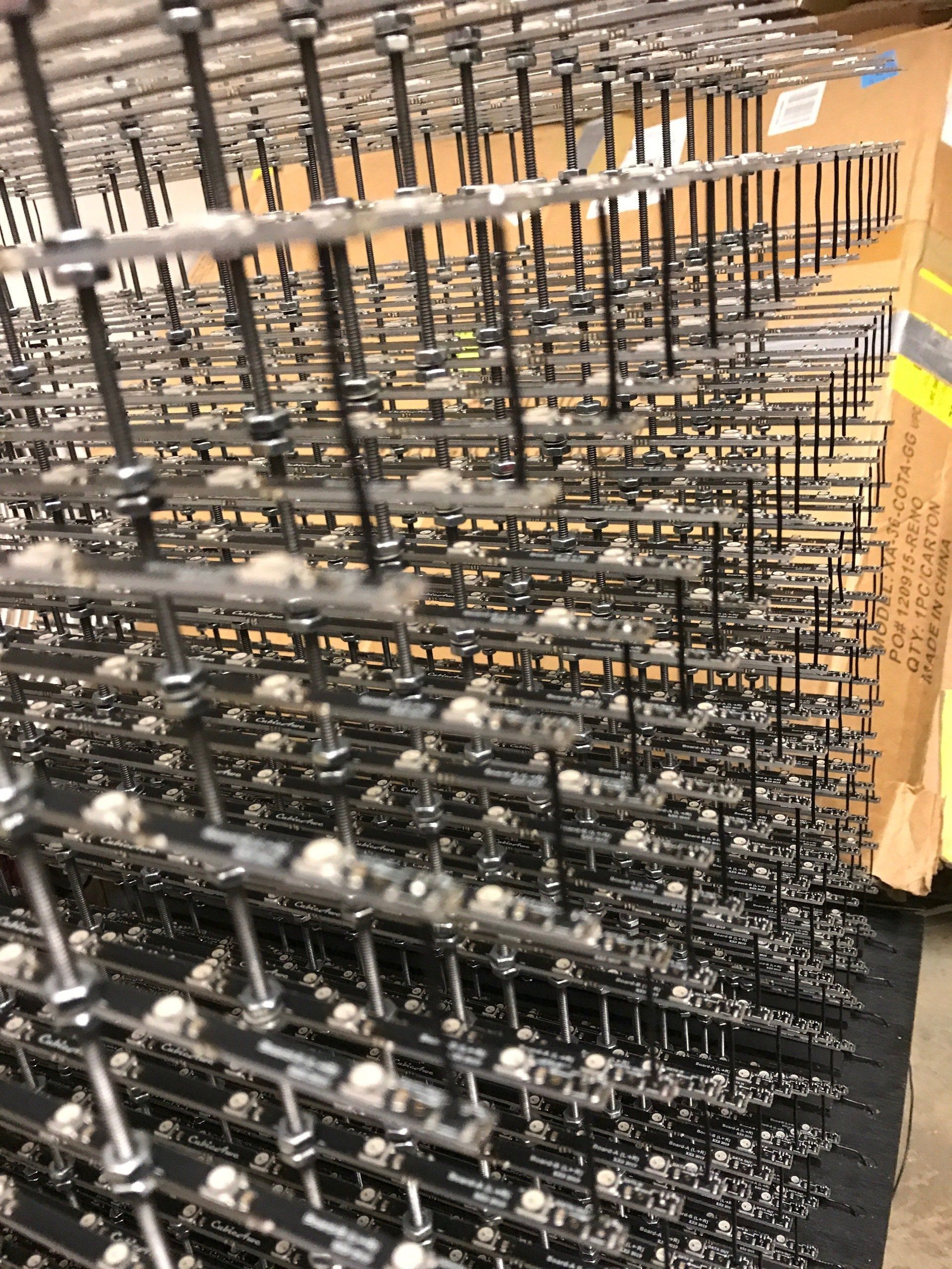
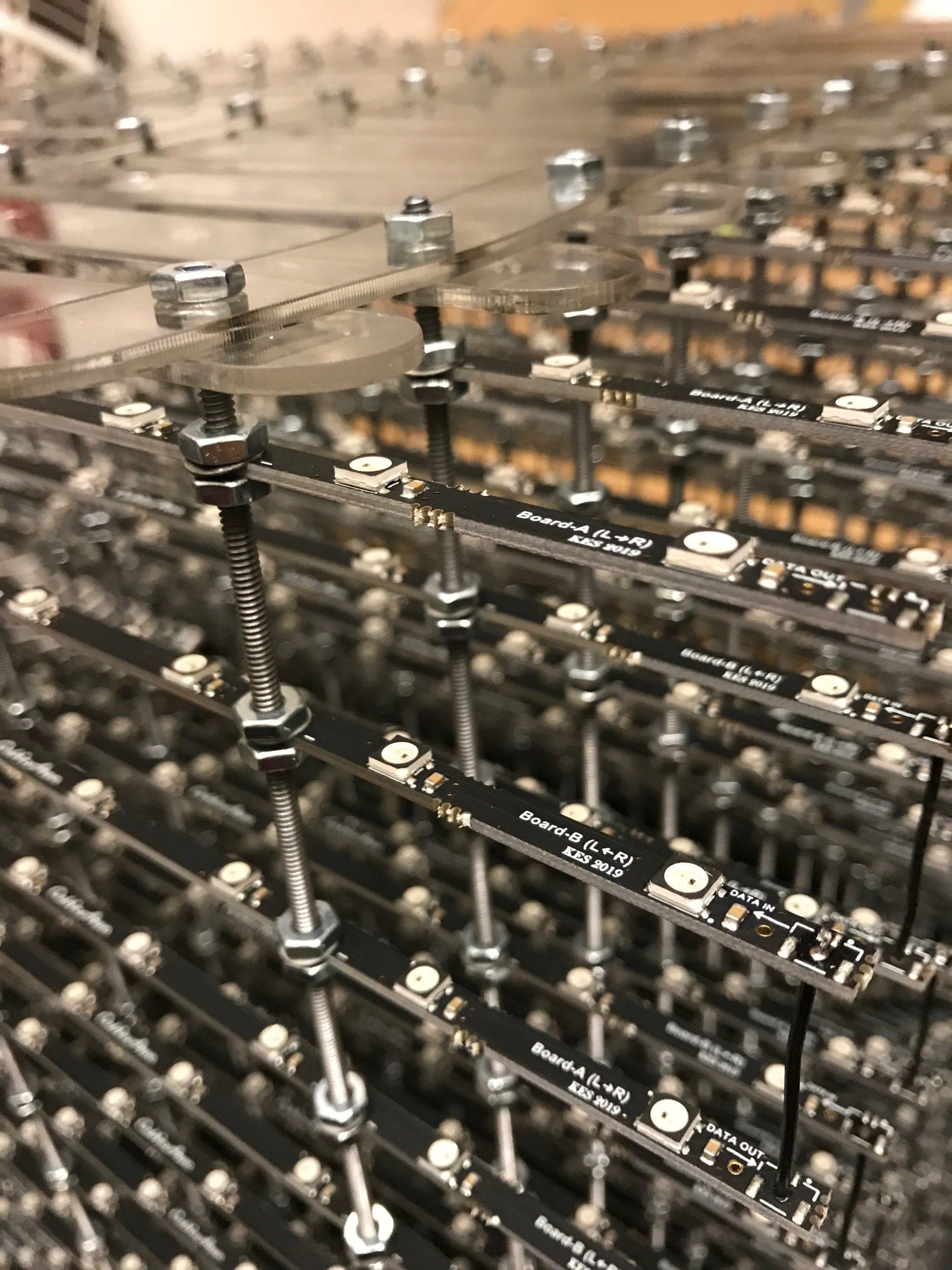
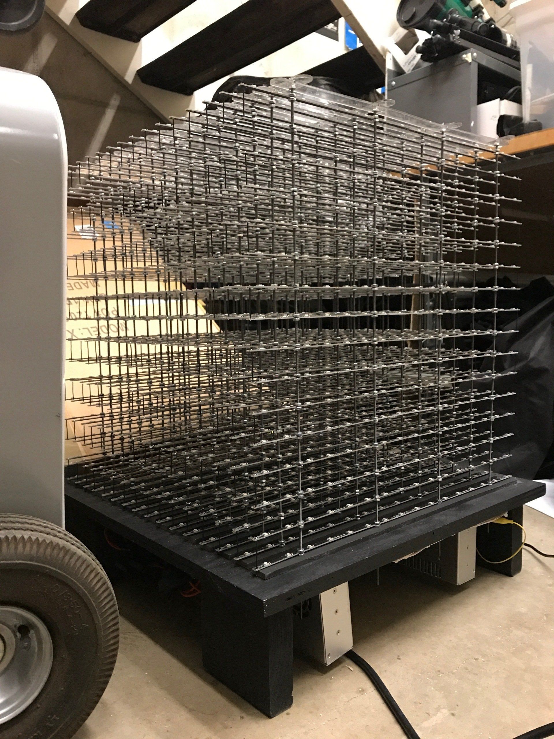
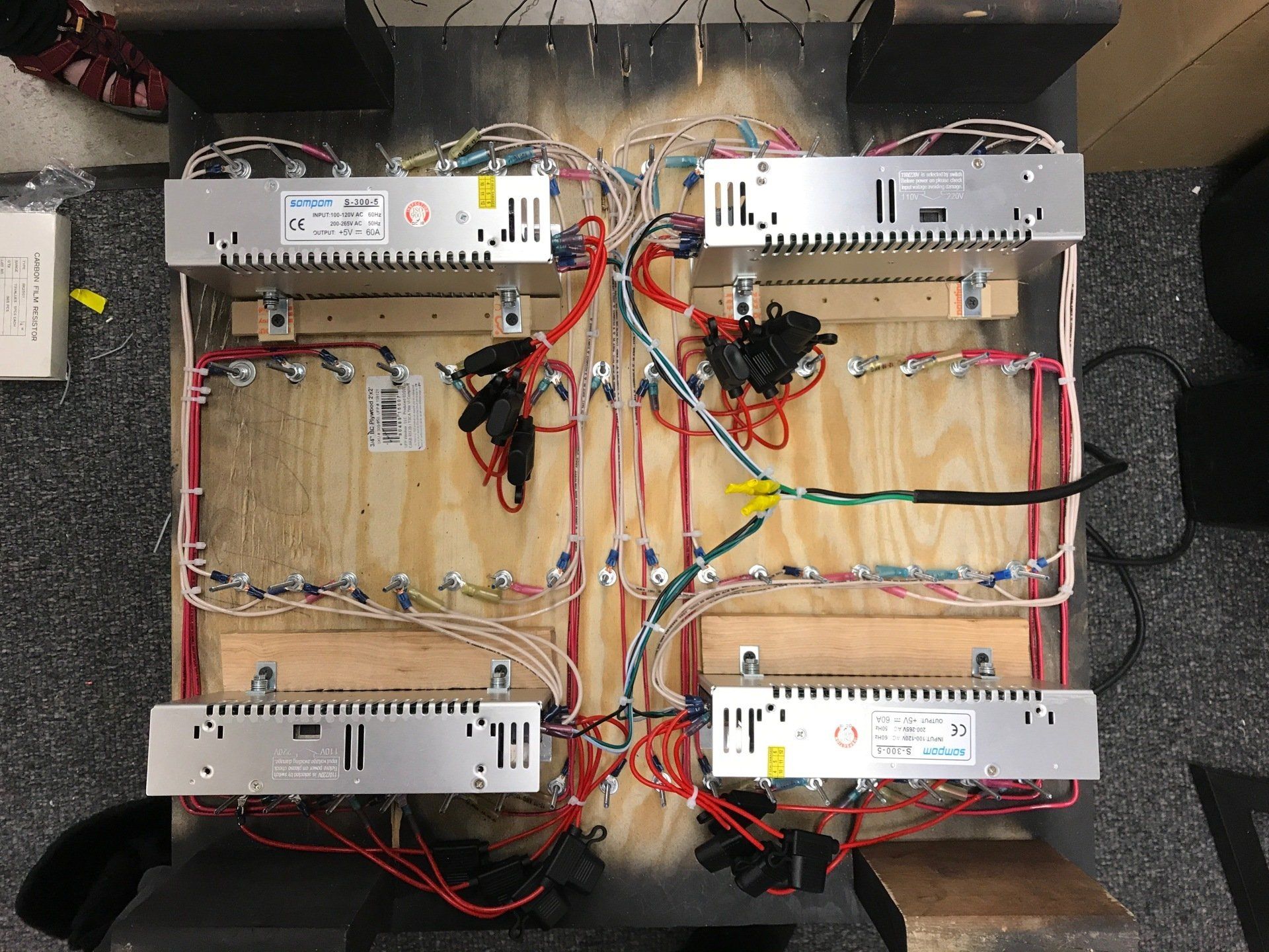
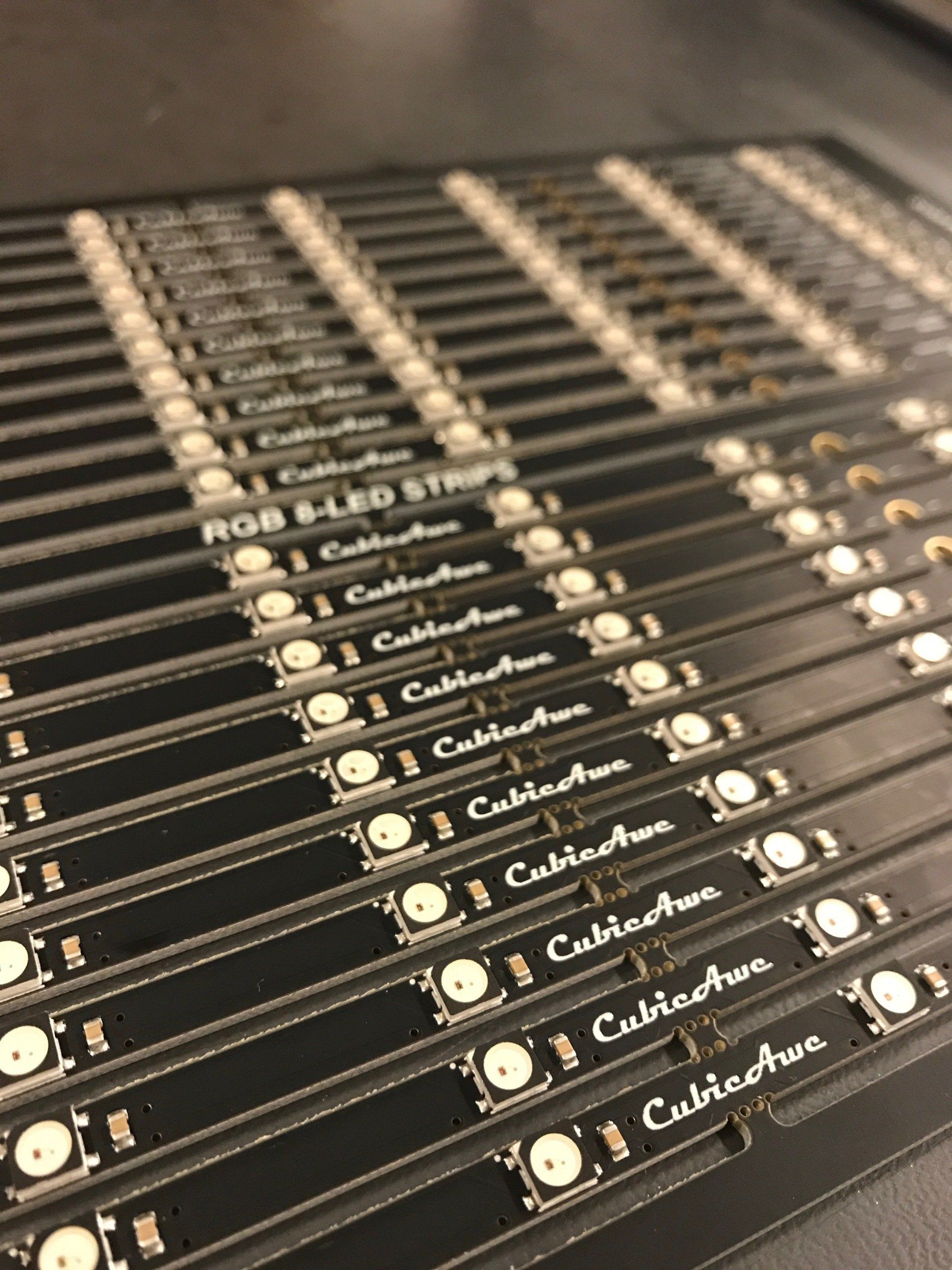
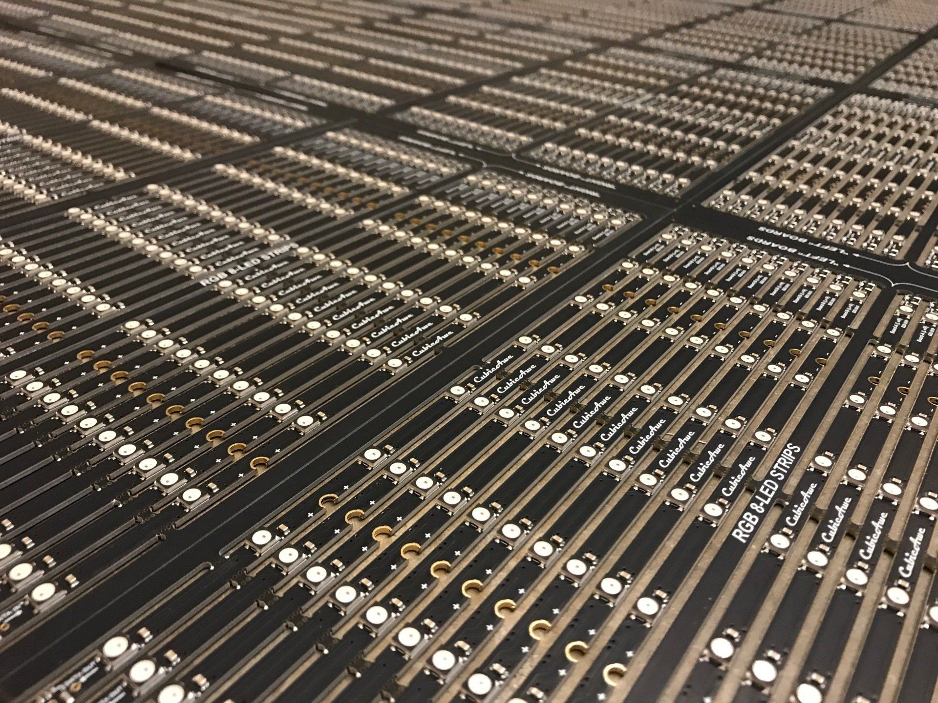
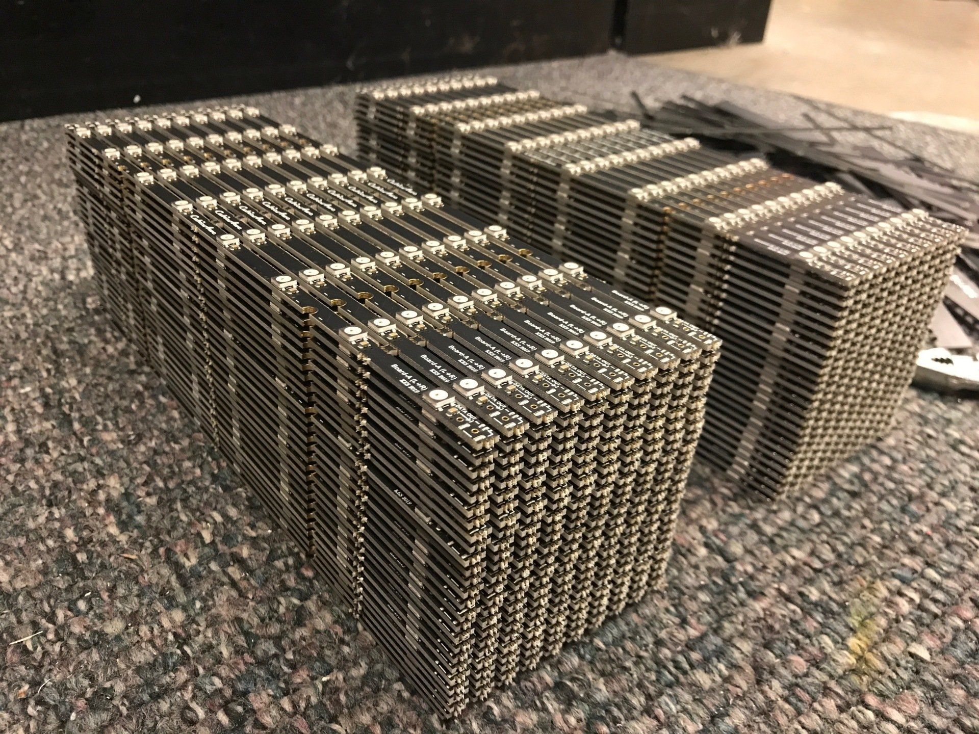
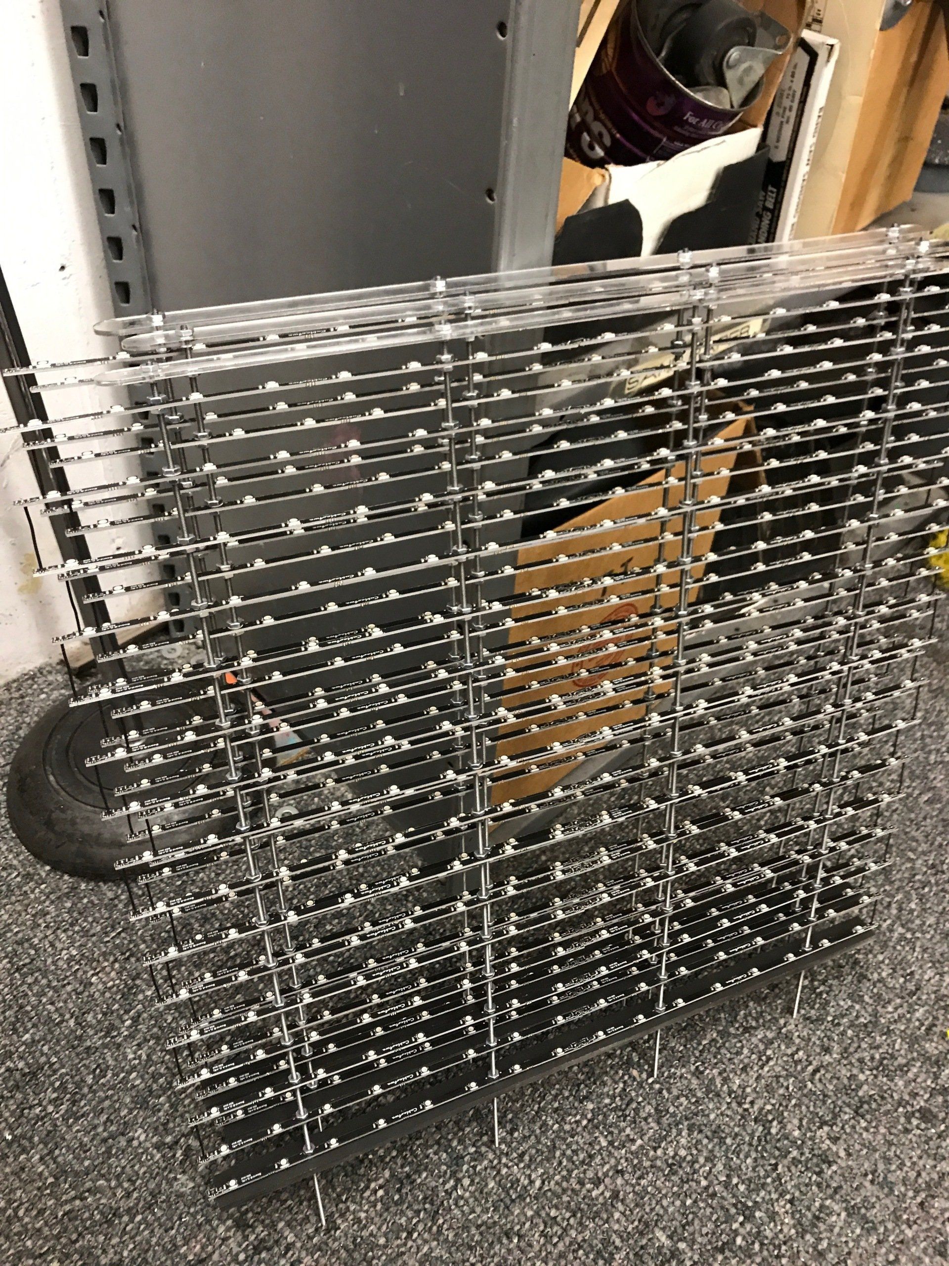
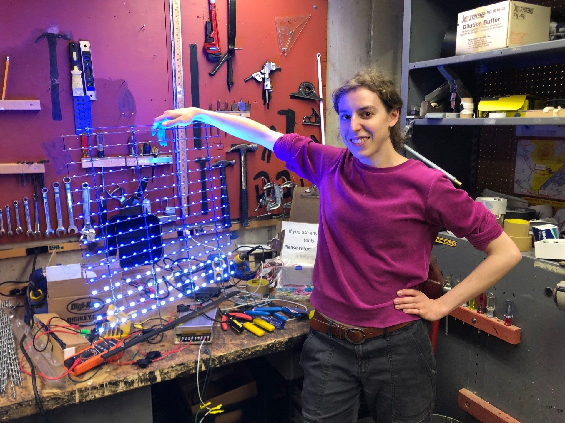
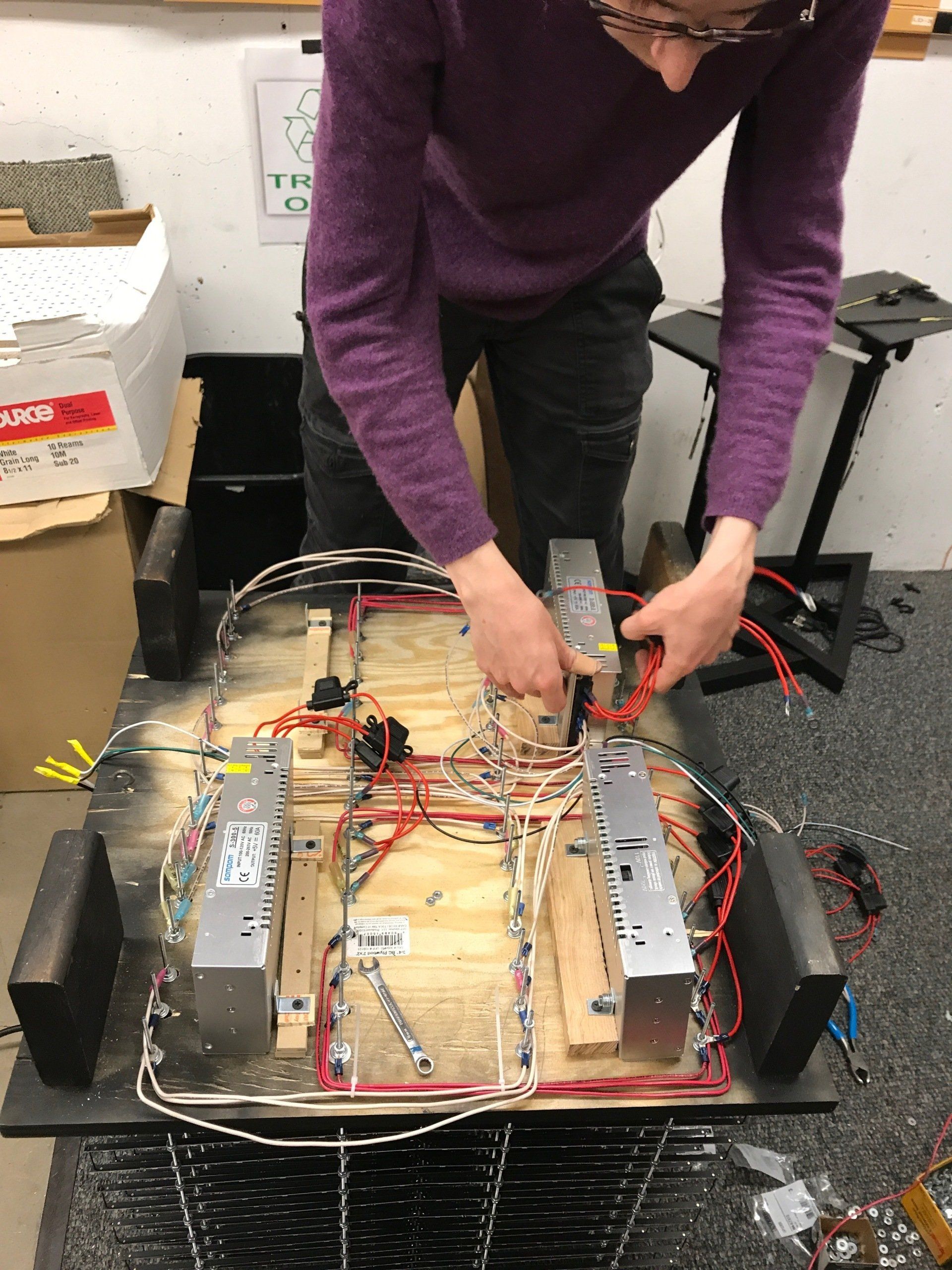
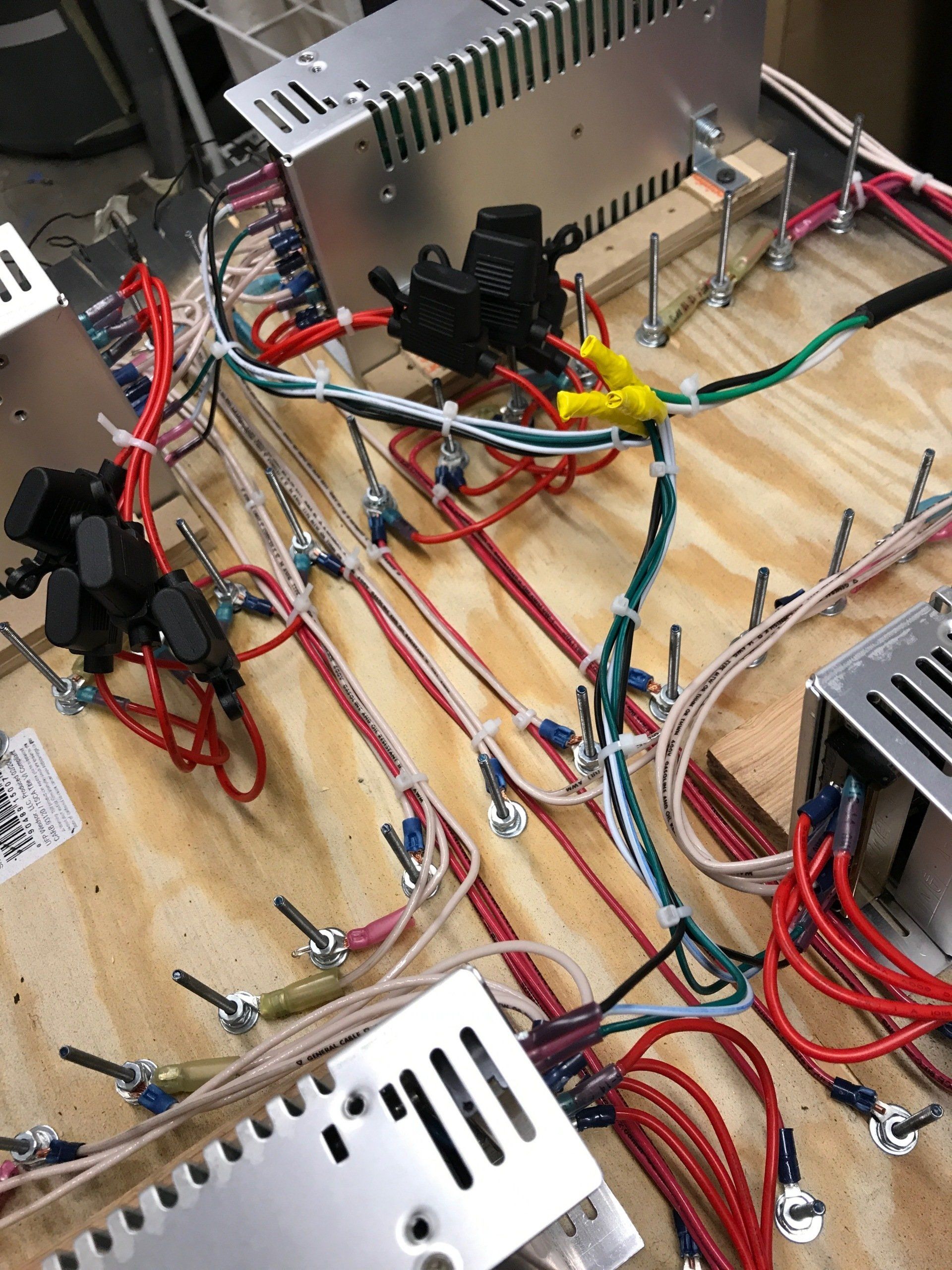
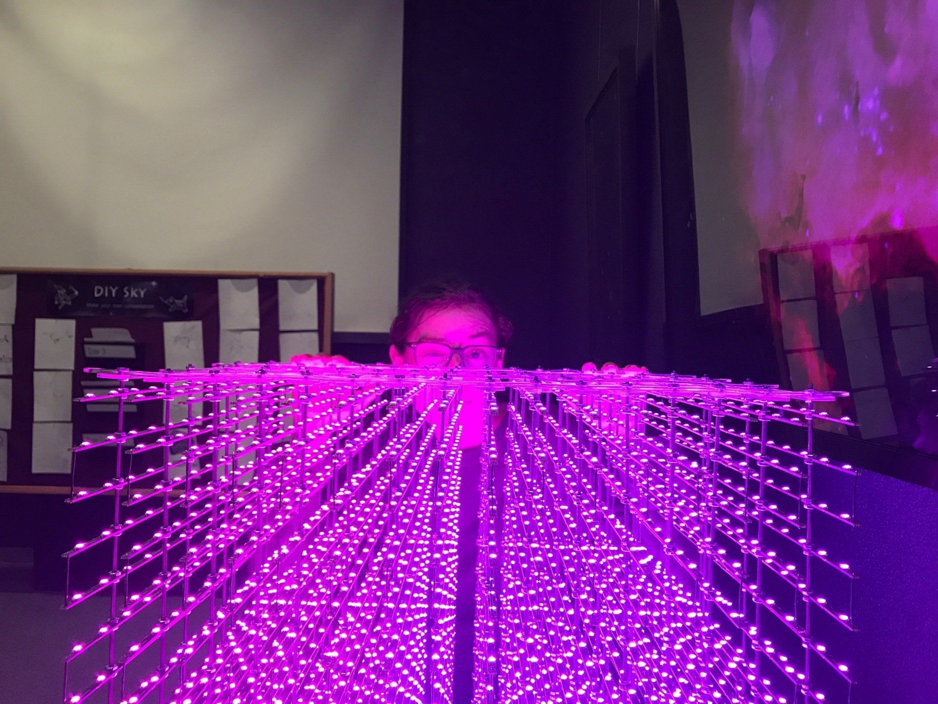
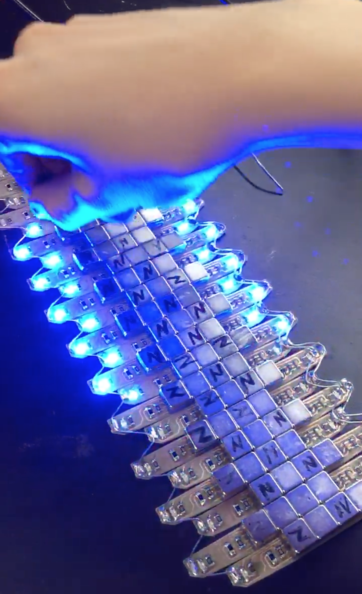
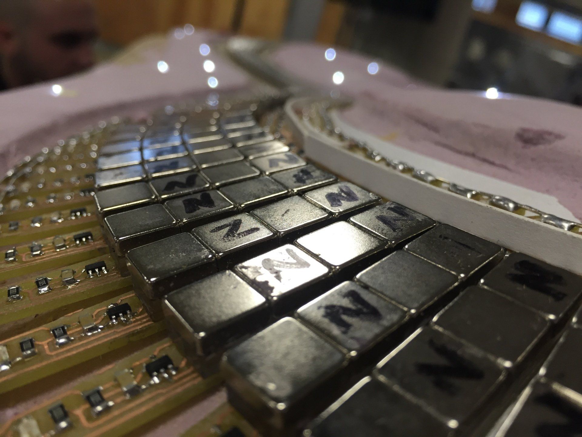
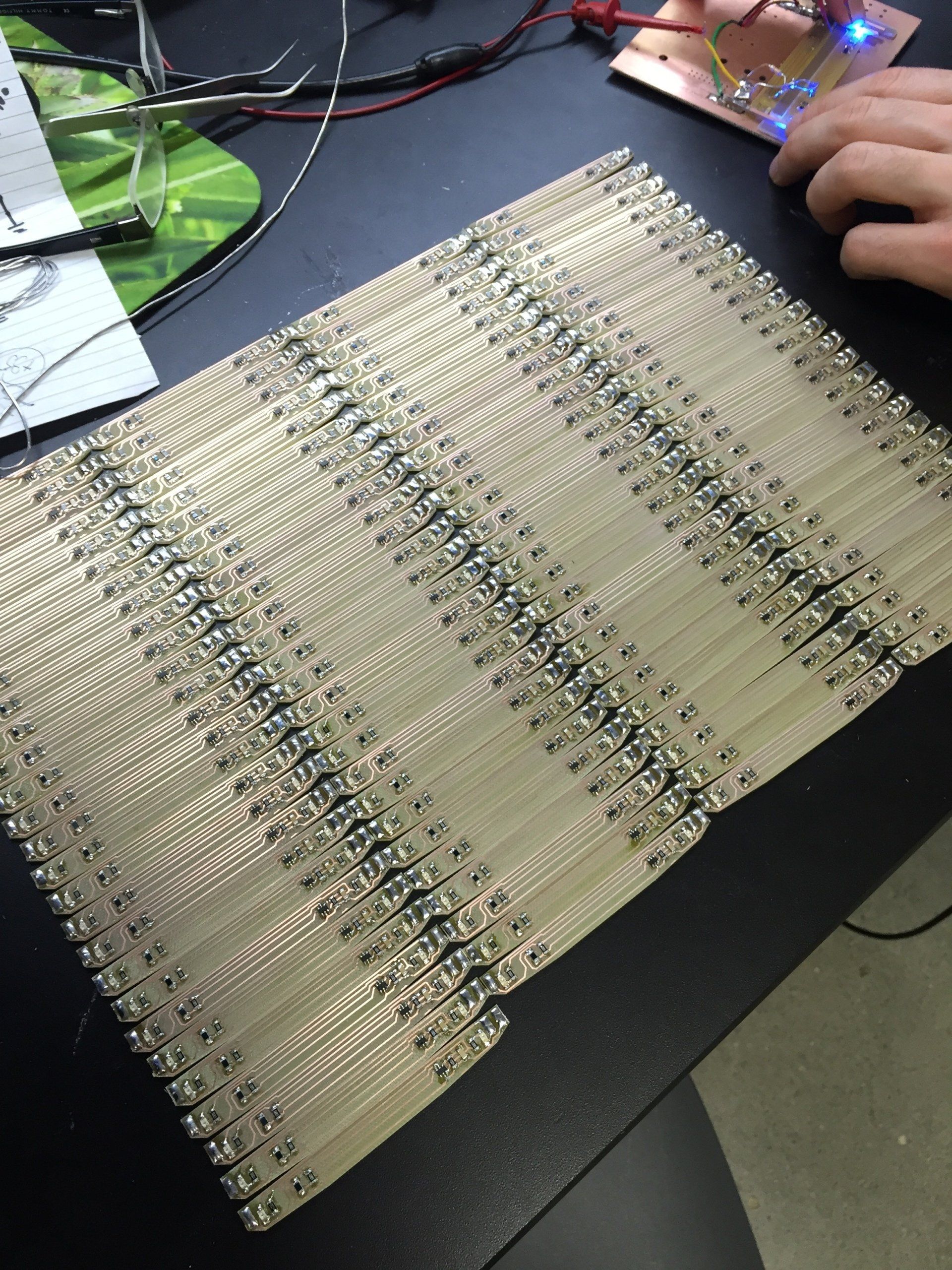
A 16 x 16 x 16 cube of RGB LEDs drawing up to 1200 Watts
I led a team of four classmates to create a 4,096 RGB (red-green-blue) LED cube from scratch within a semester, for a permanent science demo installation at the University of Colorado Boulder Fiske Planetarium. I was responsible for designing the narrow LED circuit boards and the power circuitry, as well as component sourcing and budget. Credit to Justin Trupiano for coding all the gorgeous 3D animations, Elizabeth Butler for scientific content, Bryan Constanza for designing the base, and Mikayla Costales for exhibit evaluation. Credit to everyone for tireless assembly work, and a special thank you to SparkFun Electronics and Bob Hunke for assembling the PCBs.
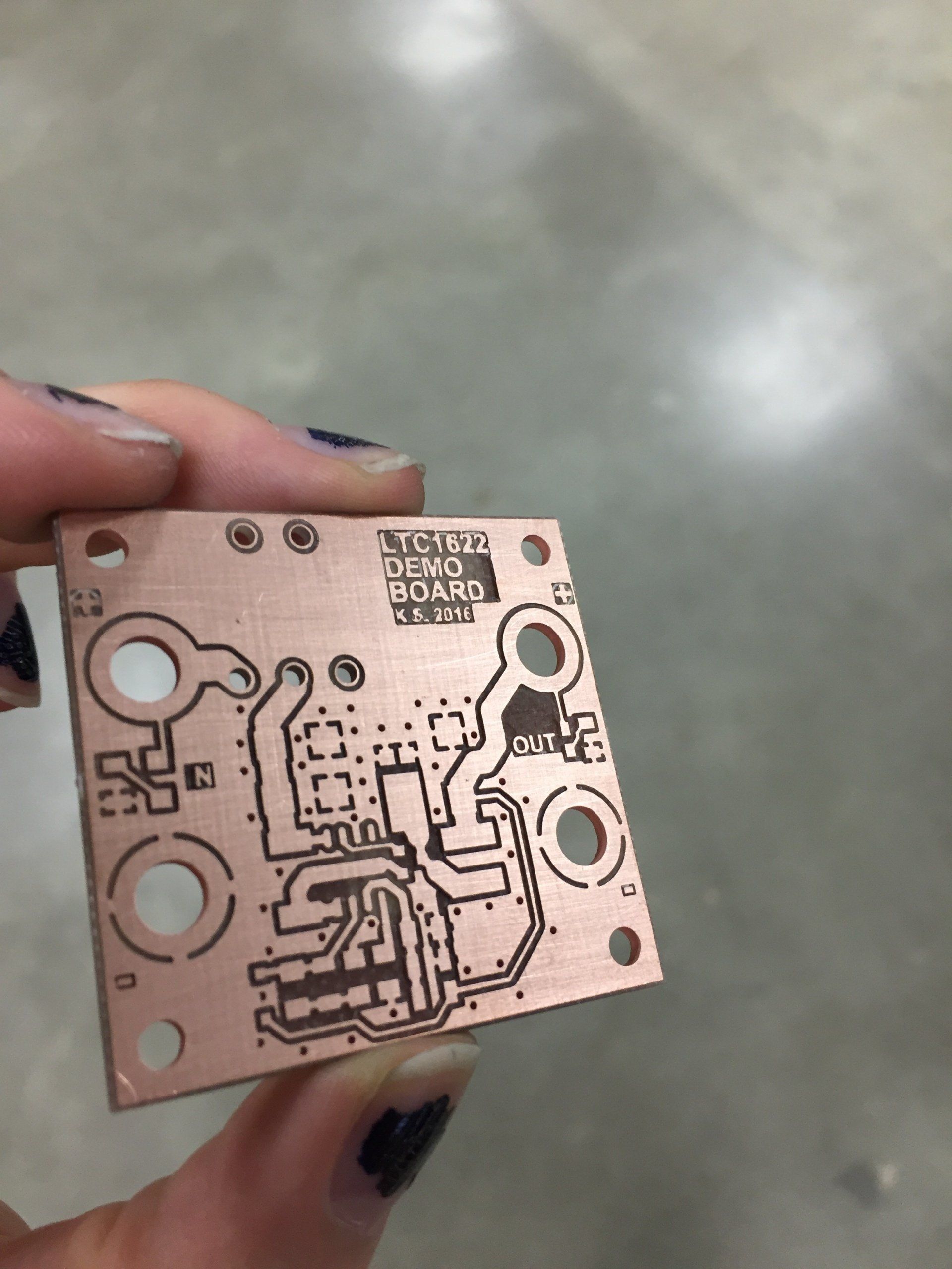
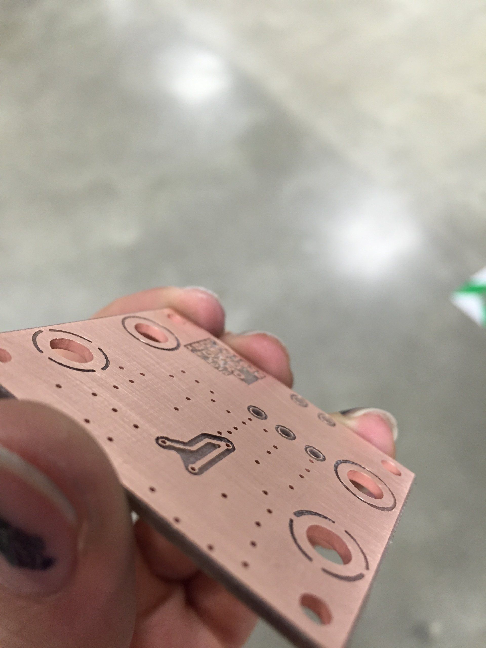
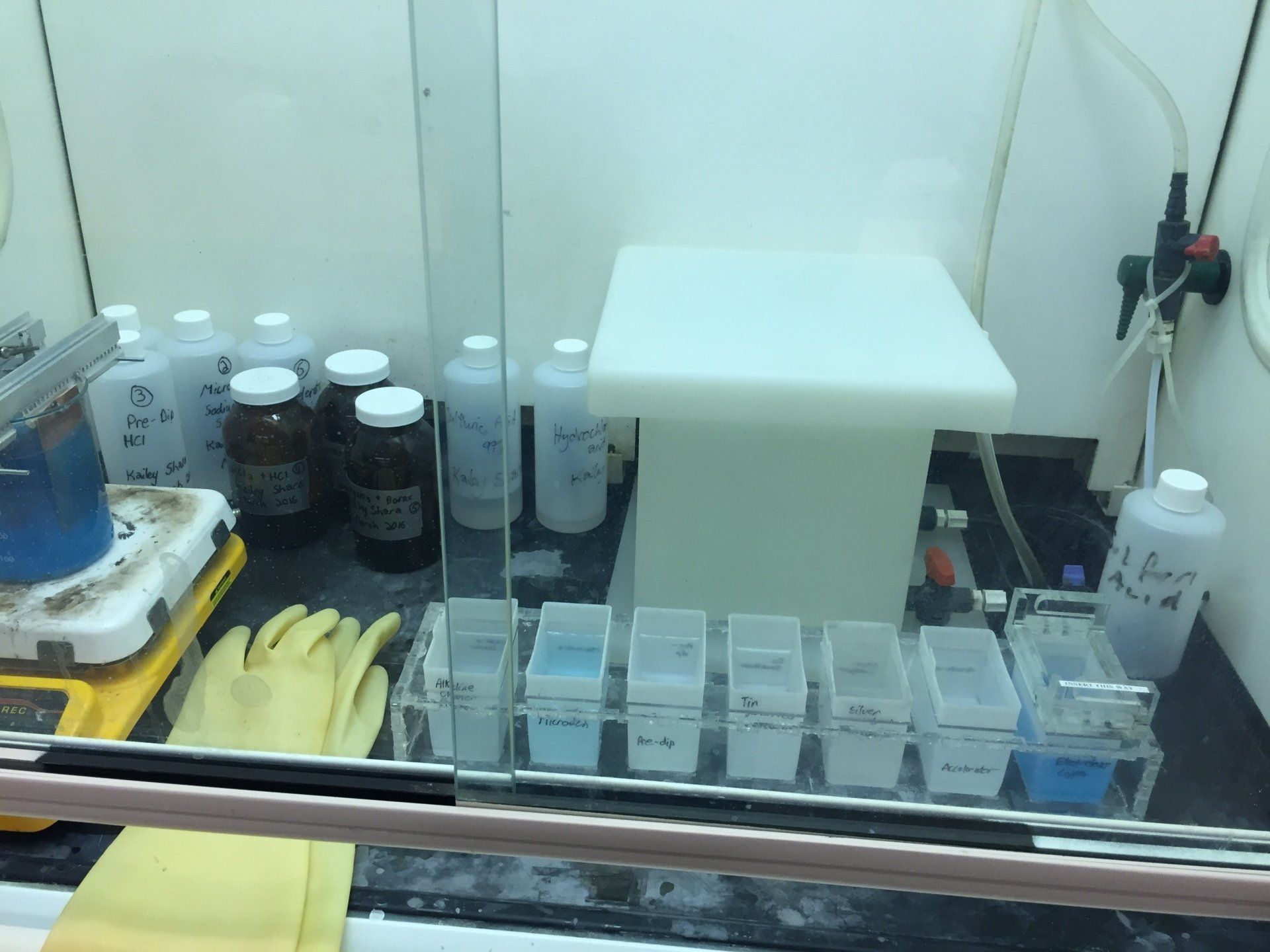
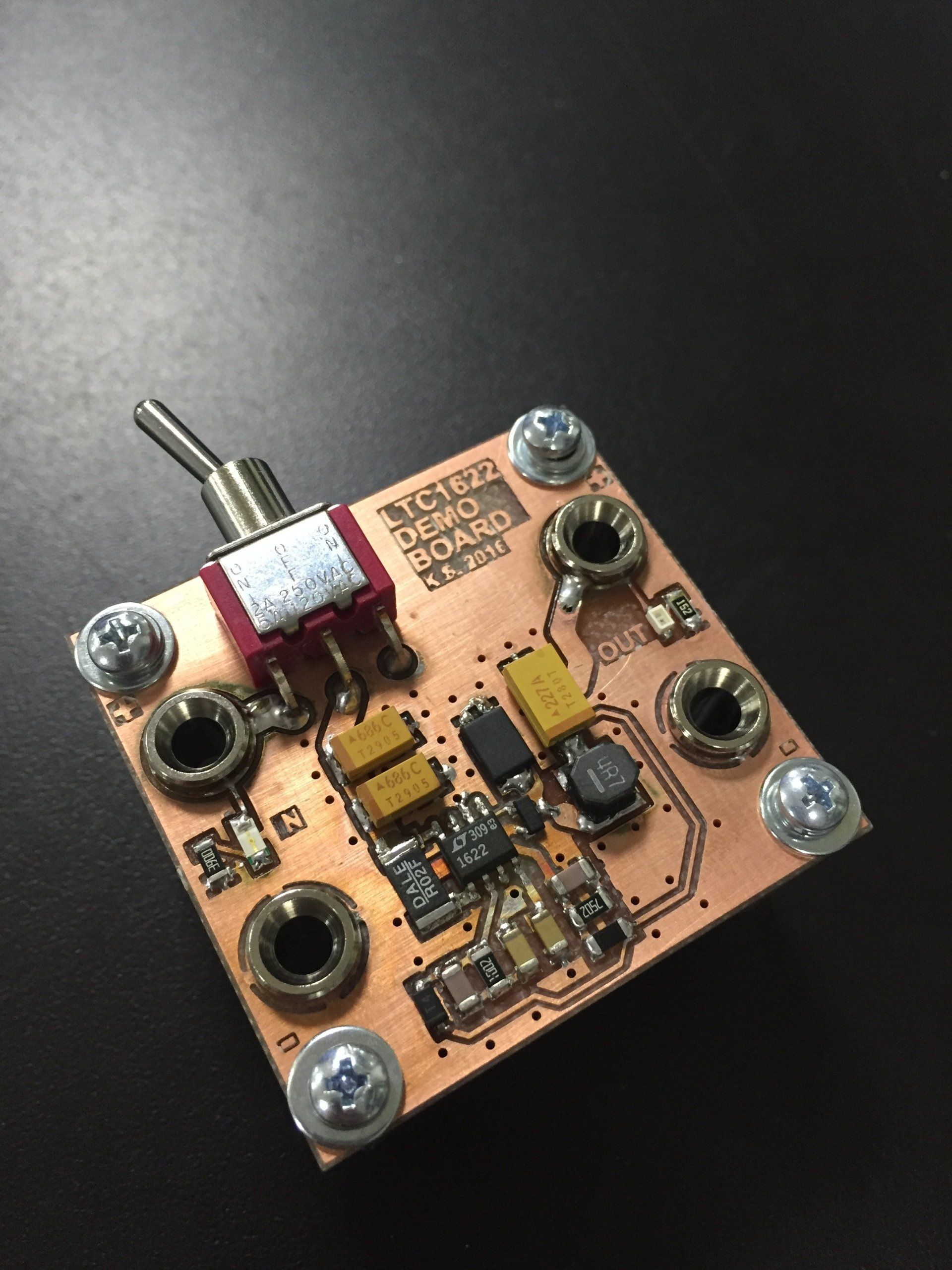
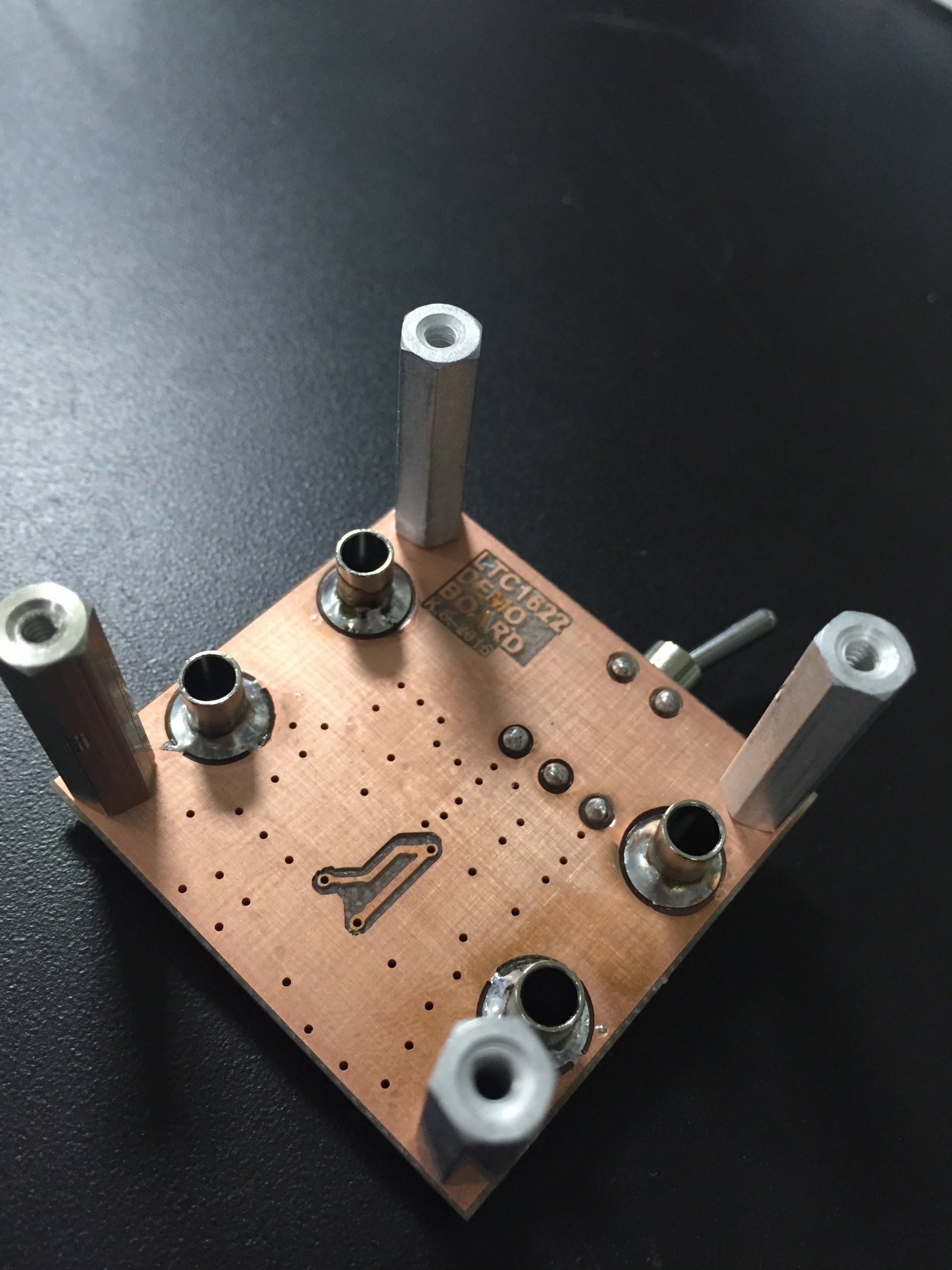
DIY Printed Circuit Board Through-Hole Plating
Making professional-quality circuit boards completely from scratch
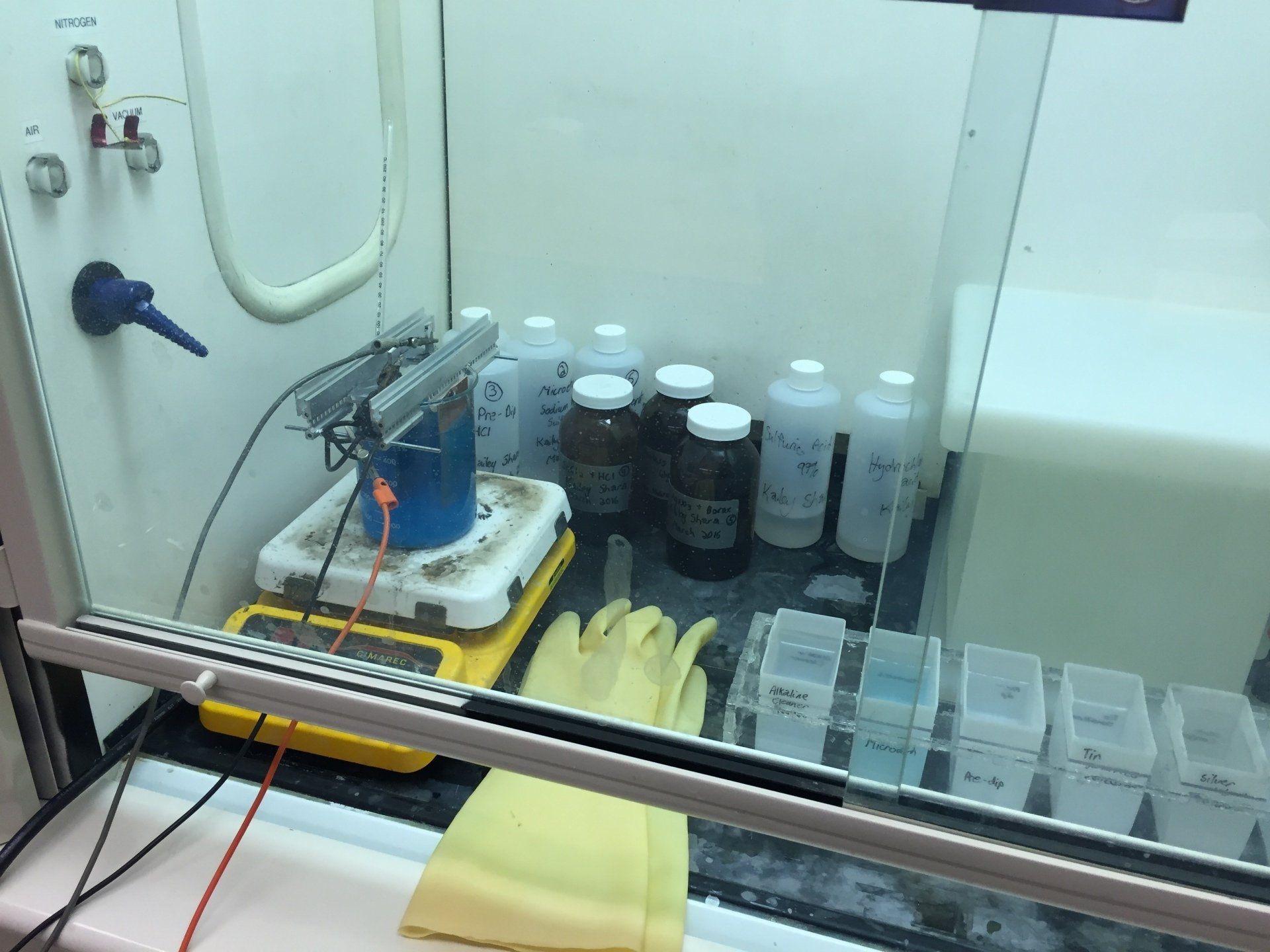
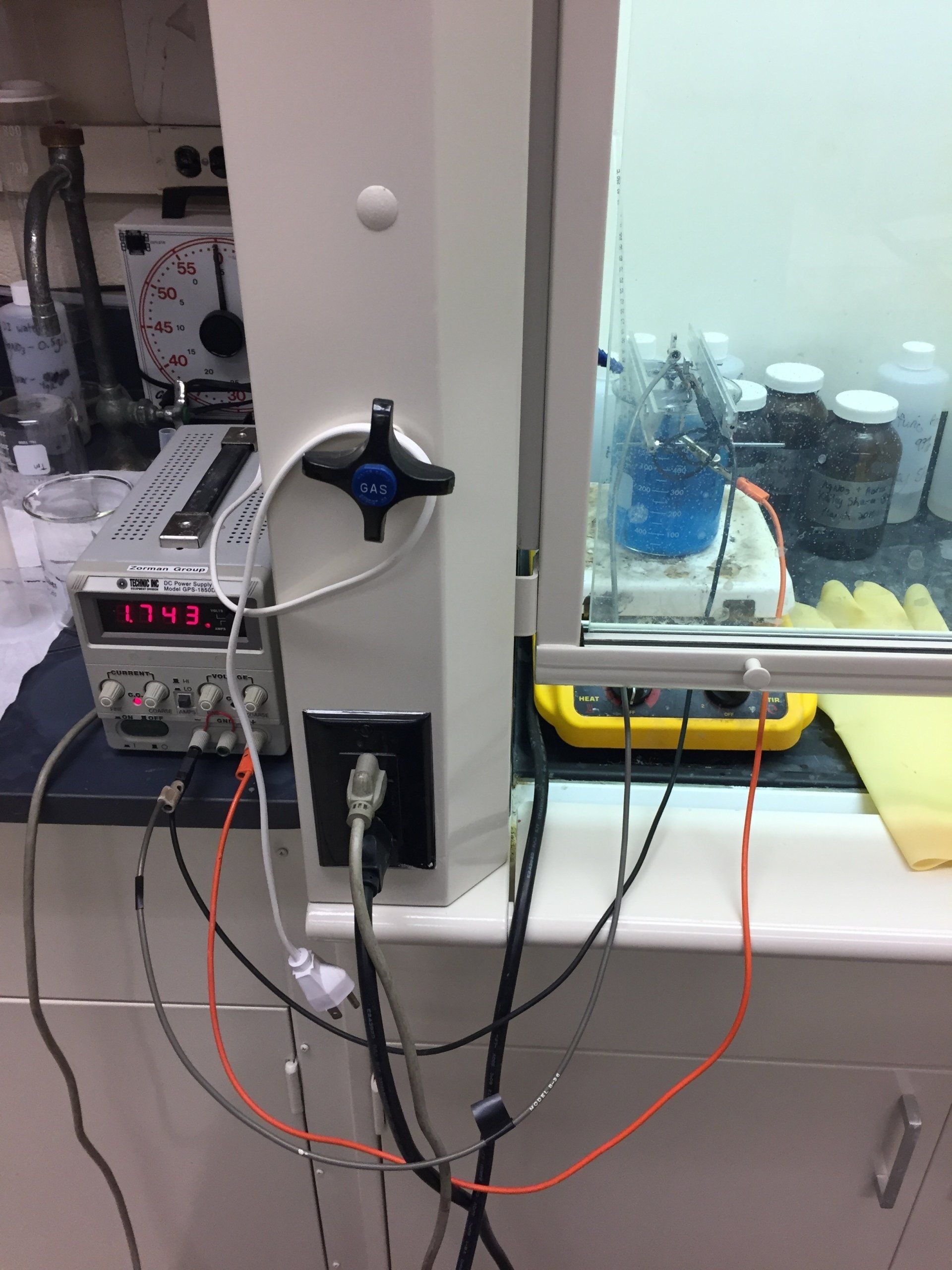
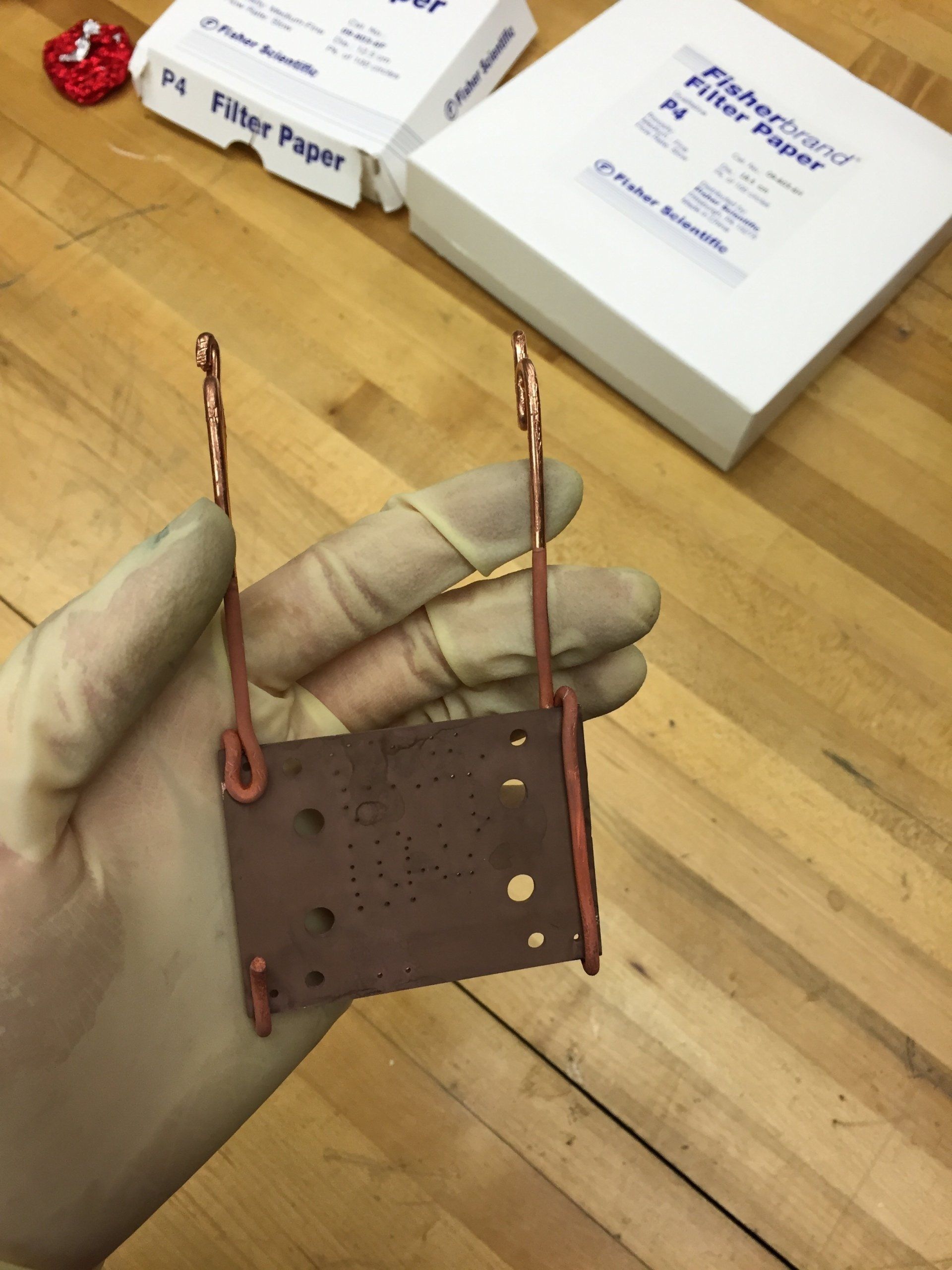
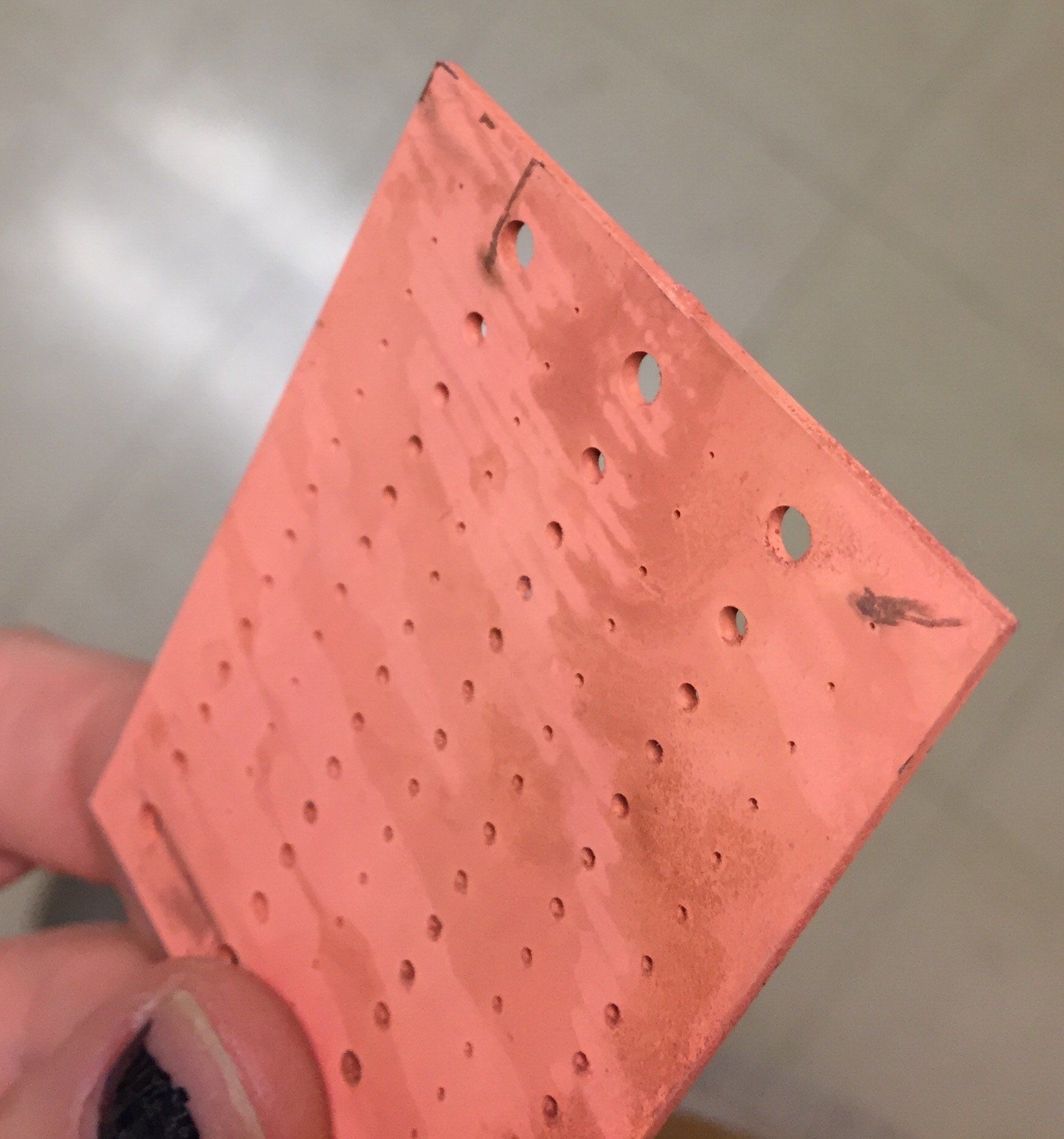
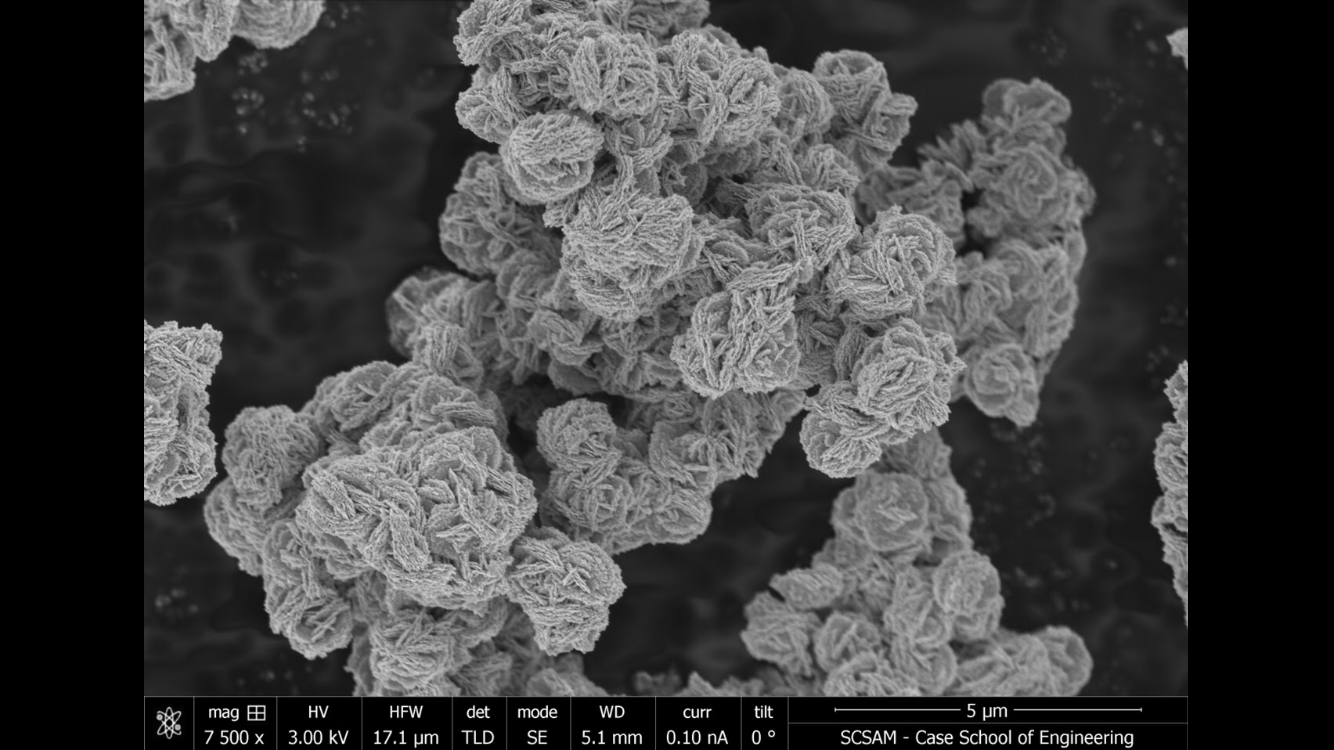
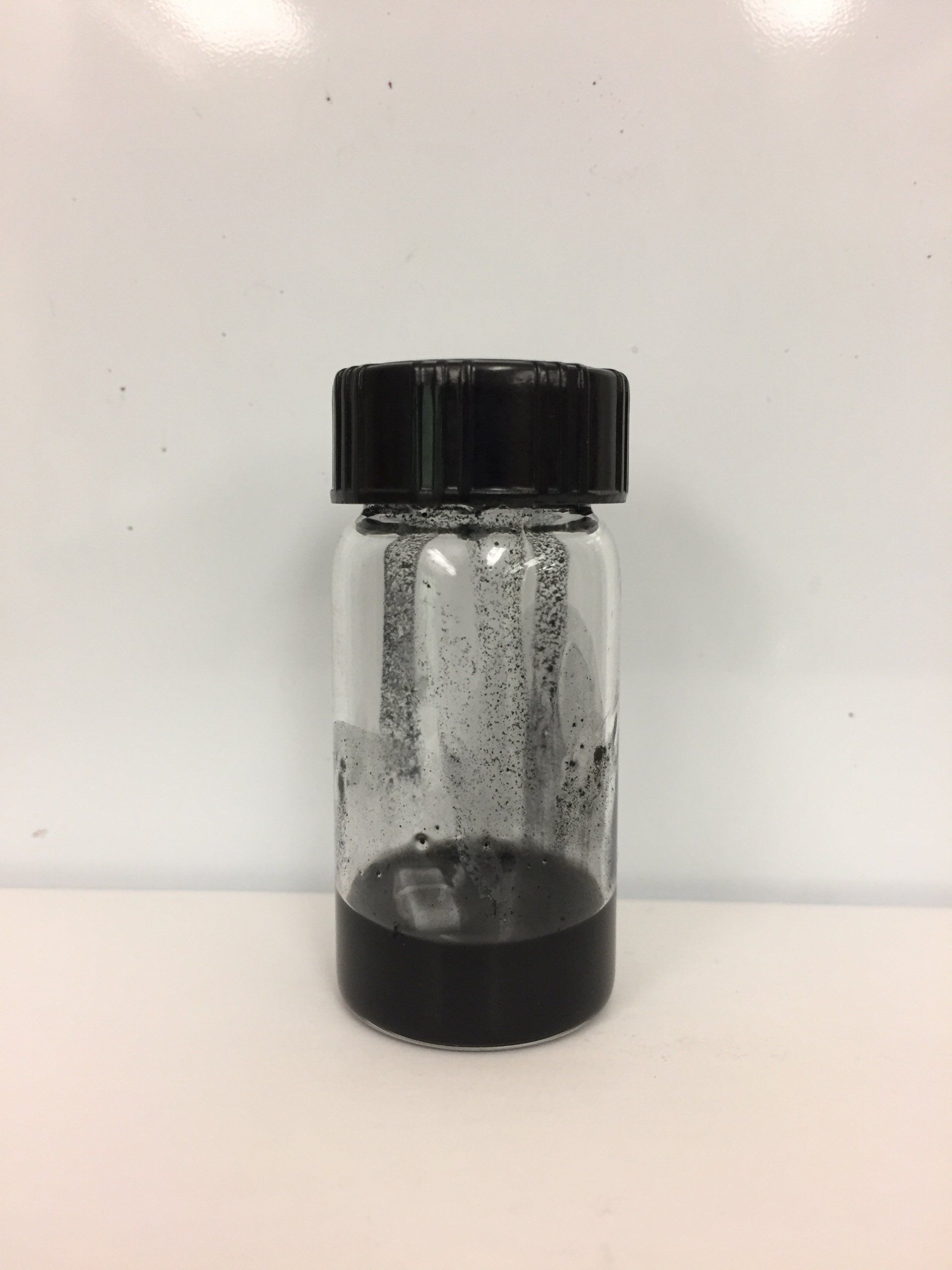
I've been making my own printed circuit boards (PCBs) going back to 2009 in my parents' basement, though only for single-layer PCBs or very simple two-layer PCBs. Electrically connecting the top and bottom layers of a two-layer PCB requires a complex but now-ubiquitous chemical process, used by all PCB manufacturers. In my second year of undergrad, I thought to myself "wouldn't it be neat to make my own two-layer PCBs?" and then spent a semester developing a working electroless copper plating recipe which would reliably deposit copper metal over nonconductive surfaces. With the help of a PCB milling machine, I made a working low-voltage power supply board with this process.
I also used the same electroless copper plating recipe in an IEEE conference paper I later published, which may be found here: https://ieeexplore.ieee.org/document/8117479
The Apollo "Everything Board" for IoT
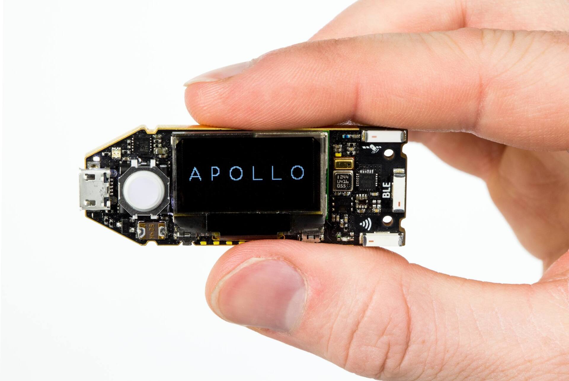
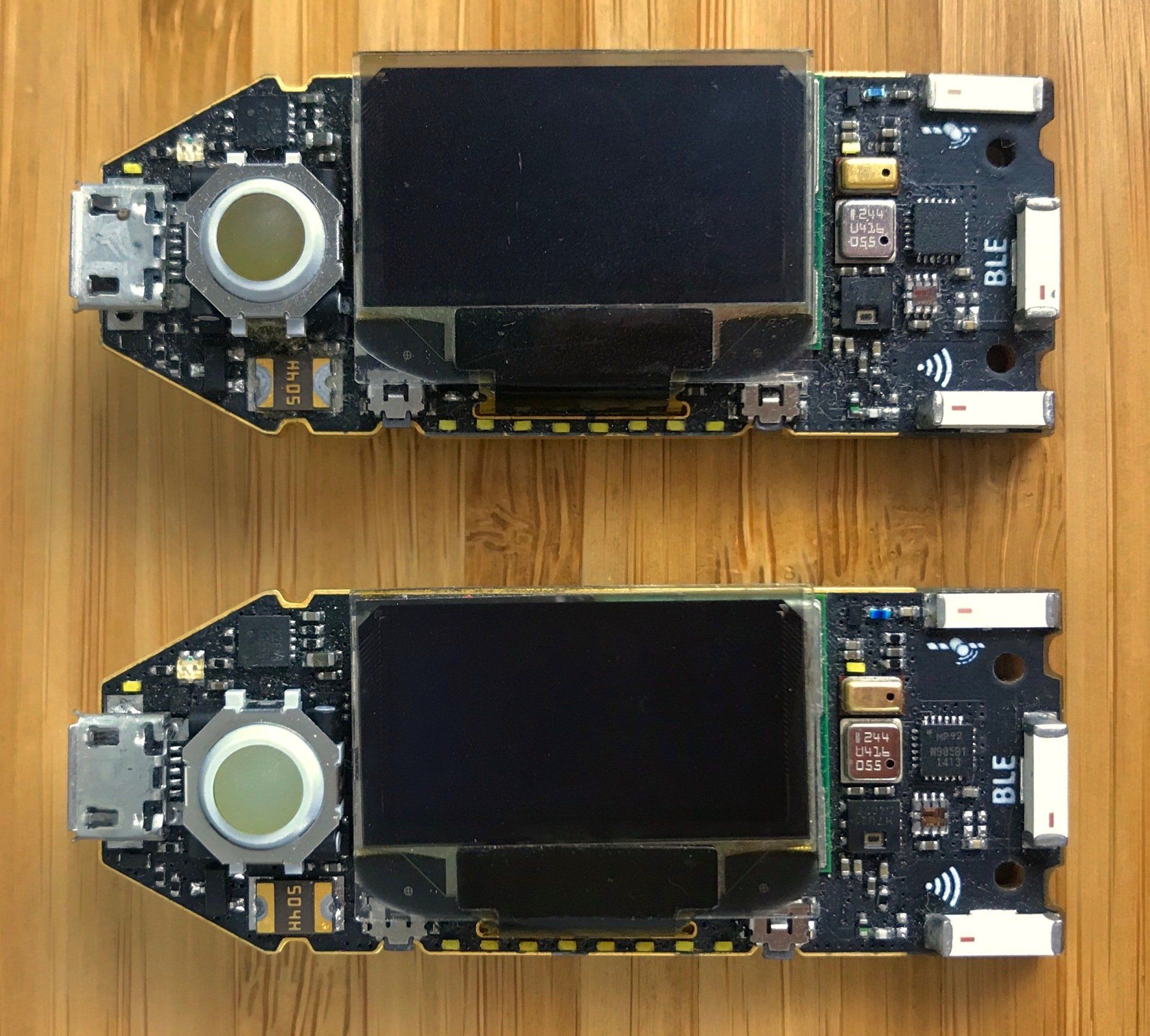
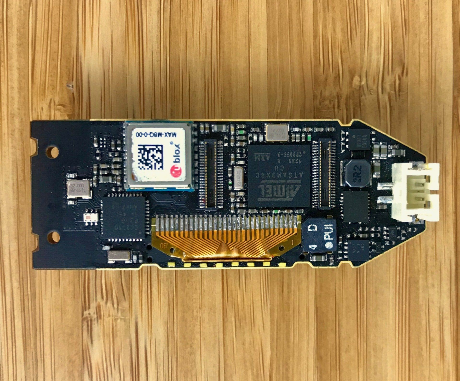
Eleven sensors, GPS, Bluetooth, WiFi, an OLED screen and a trackball in two square inches
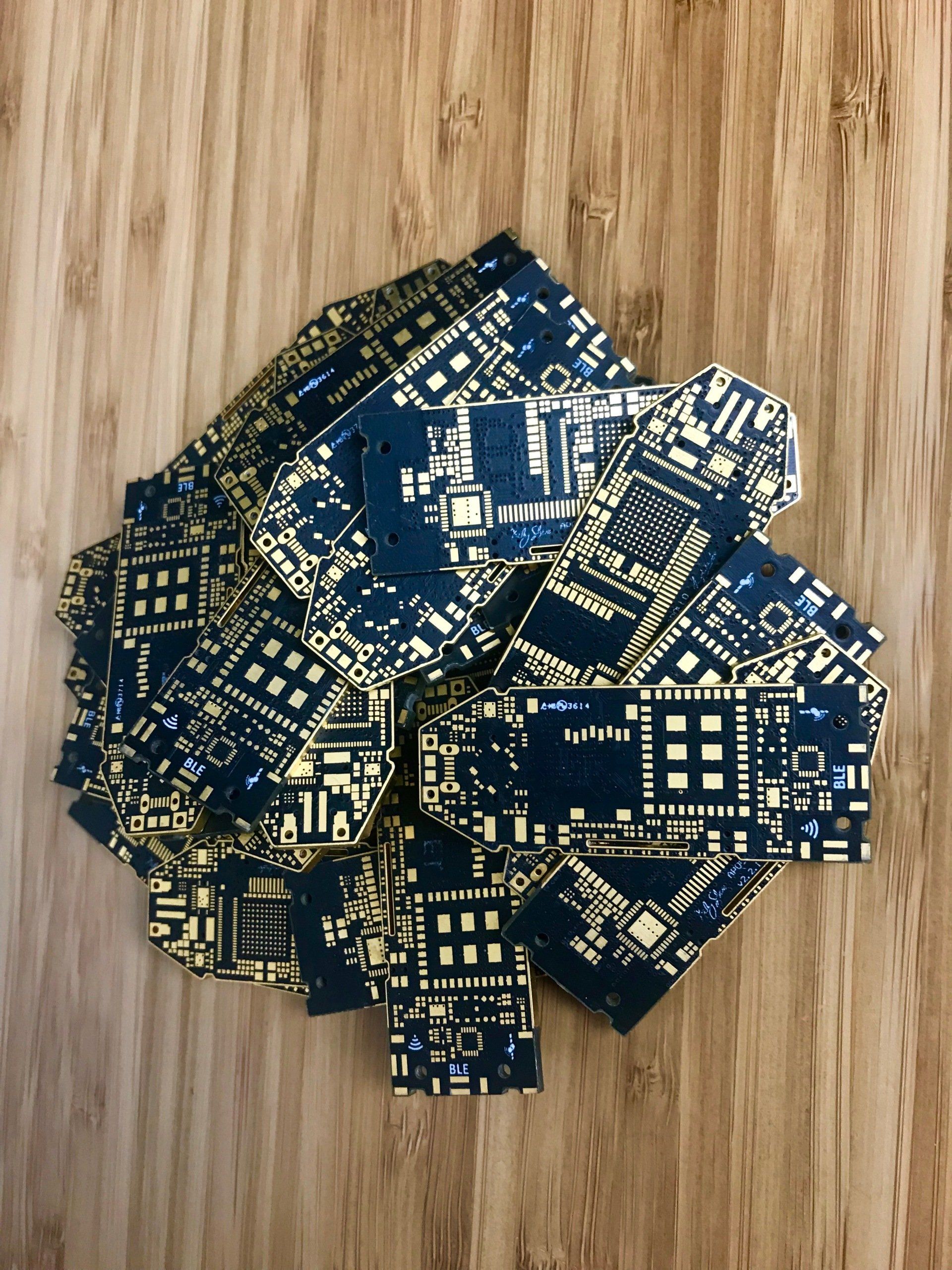
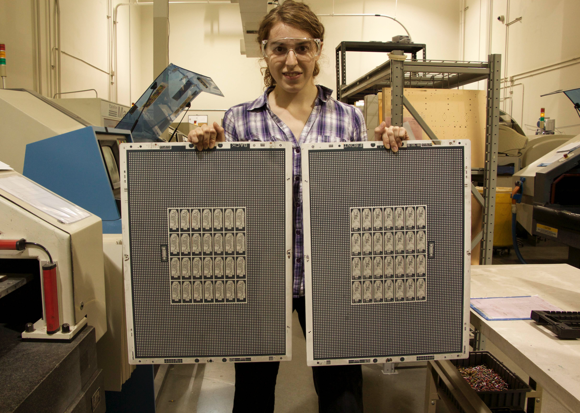
The Apollo board remains among the most complex PCBs I've designed (that I may publicly exhibit). With components on both sides, multiple radios, and severe space constraints, this was the PCB that made me proficient in Altium Designer (Altium is an industry-standard PCB CAD tool). This was routed on a 6-layer stackup, 4/4 mil rules, 12 mil vias, ENIG with matte black mask. No HDI (high-density interconnect) technologies such as blind or buried vias are used; this design uses only standard PCB technology. The PCBs were manufactured by Advanced Circuits in Aurora, Colorado. Advanced Circuits kindly permitted me into their facility to film these very PCBs being manufactured.
I assembled all Apollo boards shown here by hand with a stainless steel solder paste stencil, and reflowed in a Panasonic IR toaster oven.
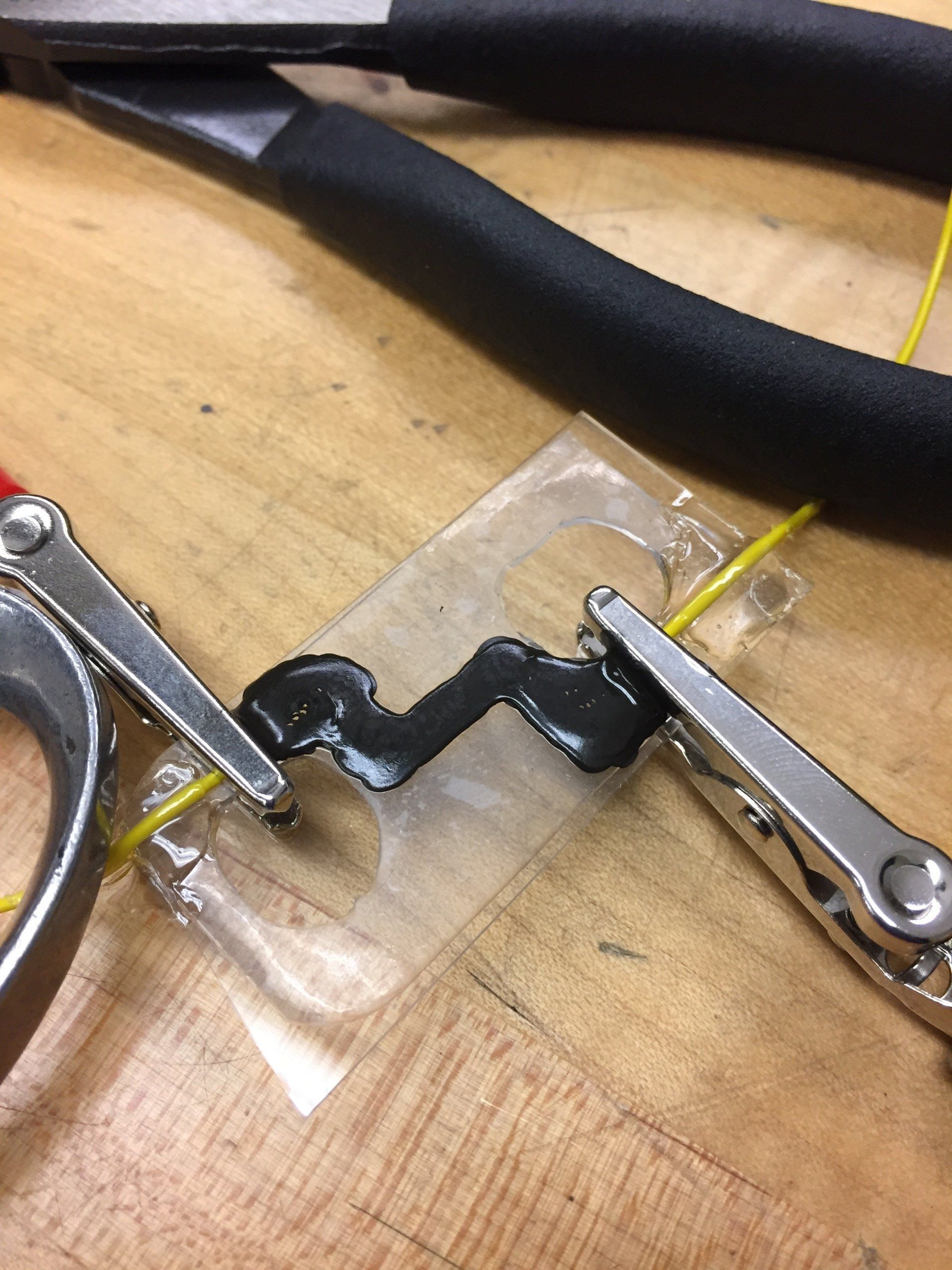
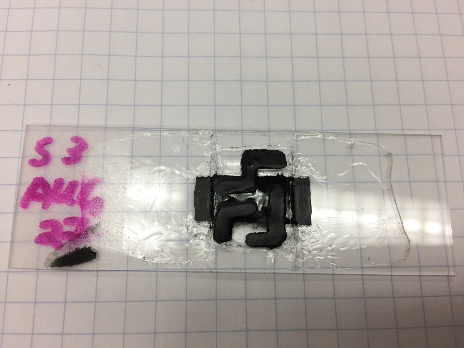
Stretchable Conductors
Elastic like a rubber band, but conductive like metal
After my electroless-copper-coated nanofibers paper, I experimented with stretchable rubber-like materials cast from inks. Stretchable conductive materials will be of particular use in wearable medical devices and soft robotics, though it's clear that these types of material system often suffer from relatively short lifetimes.
Function Generator
Build a working electronics instrument in a week
Probably my favorite class during my undergrad was EECS 371 Applied Circuit Design, still taught today by the illustrious Larry Sears. Students complete one electronics project per week for the entire semester, culminating in the design of a digital controller for a toaster. My favorite project was definitely the function generator, where our circuit had to output square, triangle and sine waveforms of variable frequency, amplitude and offset as well as a higher-current, fast rise/fall time pulse output with additionally variable duty cycle.
We were confined to the use of "simple" analog components such as opamps and comparators, and specifically prohibited from using analog switches, though mechanical switches were kosher. I liberally interpreted this to include relays, and built an extra 7400 / 4000-series digital section to handle all the signal routing between the various analog subcircuits. And made it beep when the buttons are pushed, because why not.
The Omniboard
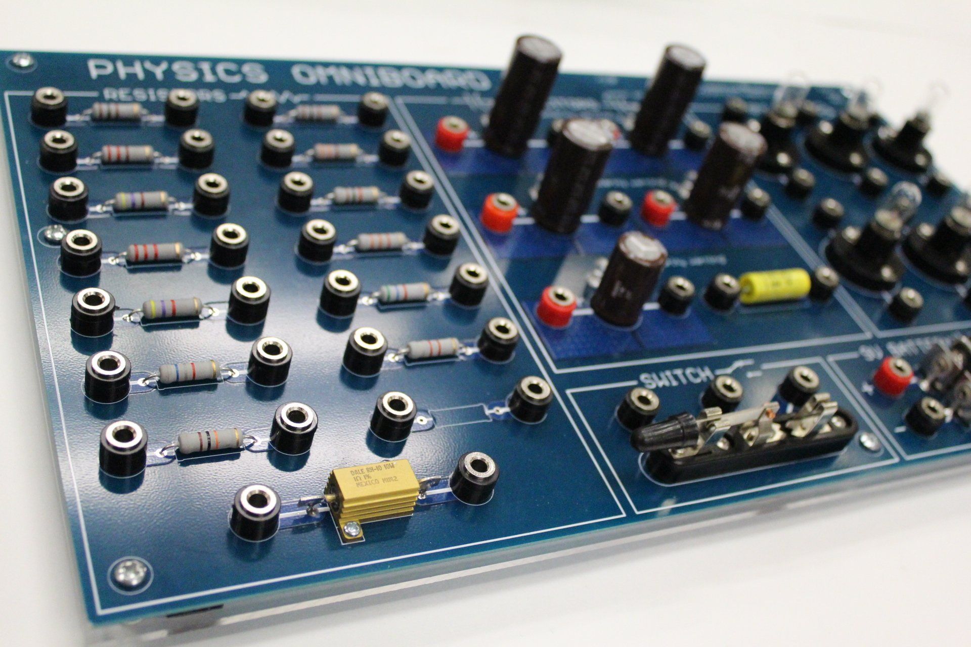
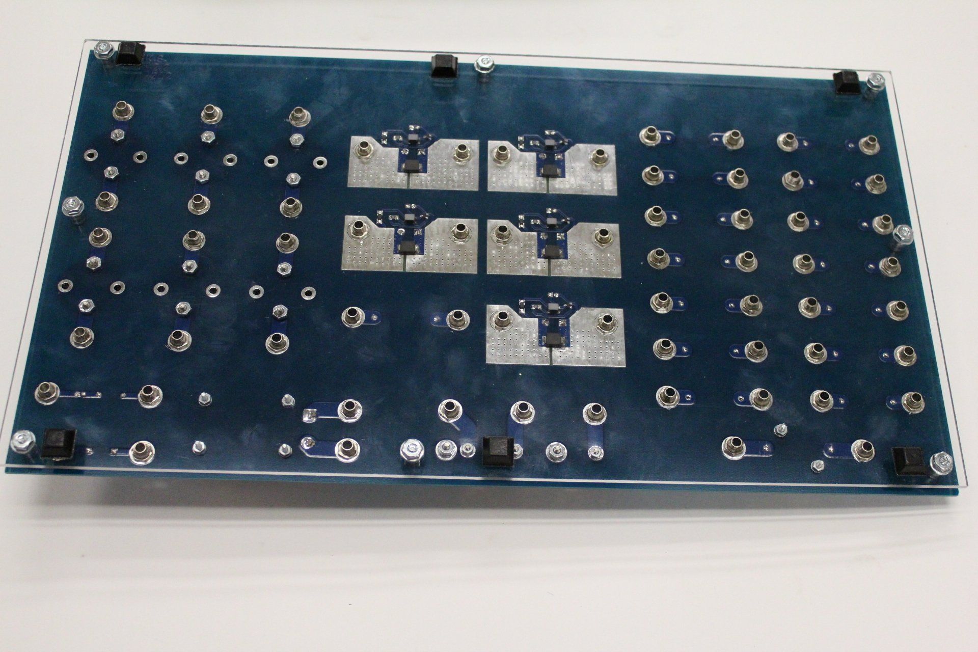
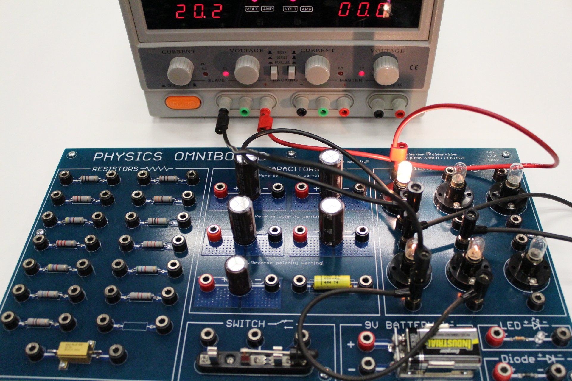
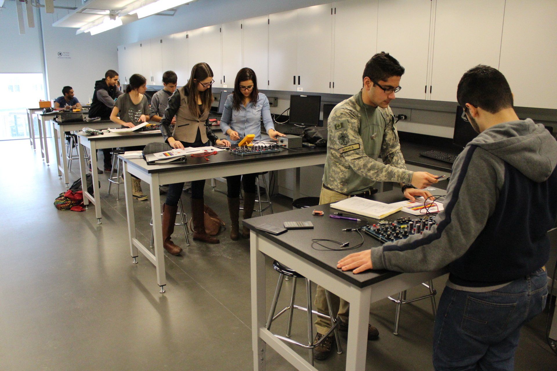
An electrical circuits teaching tool I designed and built in 2011-12, used by hundreds of students
As a student at John Abbott College in Montreal, Canada, I was hired by the Physics Department in 2011 as a part-time laboratory technician. A not completely unanimous consensus among the faculty toward adopting a more intuitive electrical circuits teaching tool was in effect. Dissatisfied with commercial options, the Physics Department elected to have the laboratory technicians construct a custom tool for wiring together simple electrical circuits, for use in the electricity and magnetism teaching labs. I enthusiastically started work on the project with one of the two lab techs. Not longer after, this lab tech sadly suffered a very sudden stroke; although he survived, it would be many months before someone would be hired in his place, and the project became de facto my responsibility.
Making fifteen academics happy about changing a core tool used in the class they teach is generally difficult, but I made sure that every single instructor had a say in my design. Multiple prototypes later I finally went into "mass production", assembling thousands of surface mount, though-hole and mechanical components by hand across the 28 units I was building. They went into service in fall 2012, and despite significant electromechanical abuse over the years, are still going strong today.
Although the engineering behind this project was much simpler than in most of my other projects, the feeling that I left something of myself behind in direct benefit to future generations of students has always stuck with me. It also helped me win a substantial scholarship to Case Western Reserve University, which quite literally changed my life, and for which I remain extremely grateful.
Makerspace Demo for Adam Savage
Hundreds of LEDs lighting the trail to a levitating Millennium Falcon
In just about the most complicated and entertaining way possible, a small team of dedicated artists and engineers welcomed Adam Savage of Mythbusters fame to Case Western Reserve University's makerspace, Sears think[box].
I was tasked with illuminating a trail of blue LEDs behind a mini Millennium Falcon model as it passed above a "track" of magnets; the Millennium Falcon levitated by means of a liquid-nitrogen-cooled YCBO superconductor disk. Each "segment" of LEDs (one on either side of the track) is triggered by infrared (IR) light, and an IR LED was carefully positioned on the underside of the Falcon. The blue LEDs switch on immediately when the Falcon's IR LED passes over a phototransistor, but then turn off slowly. The decay time constant is adjustable by means of a "third rail" common to all 200 or so "segment" PCBs with an externally-applied voltage. Thus, by changing the applied voltage, the LED light persistence may be adjusted up or down, and therefore the length of the blue LED trail is lengthened or shortened.
Credit to Ian Charnas for organizing the project and leading the team. Detailed credits at the end of the video below.

Transistor Decade Counter
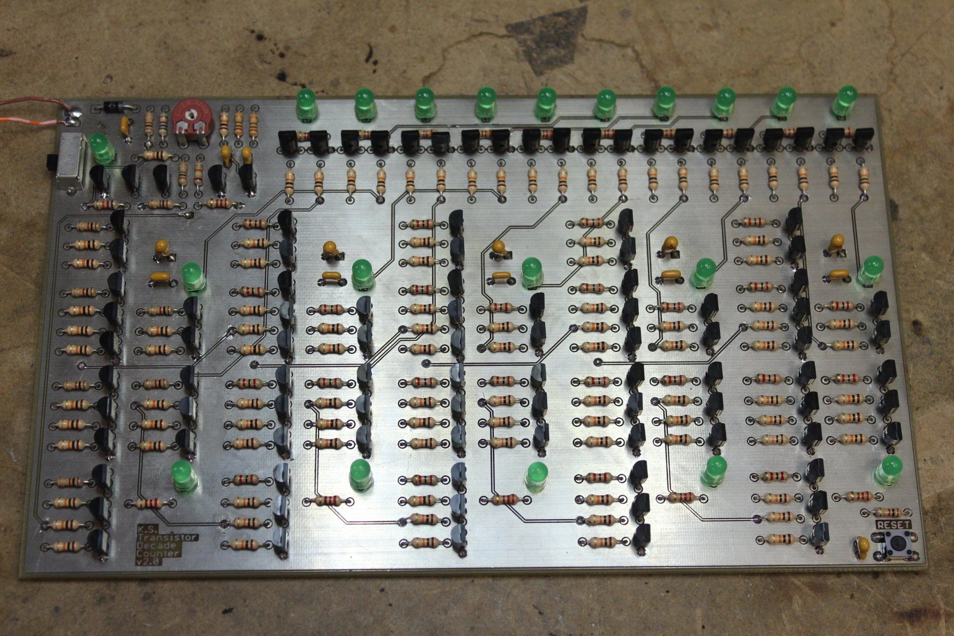
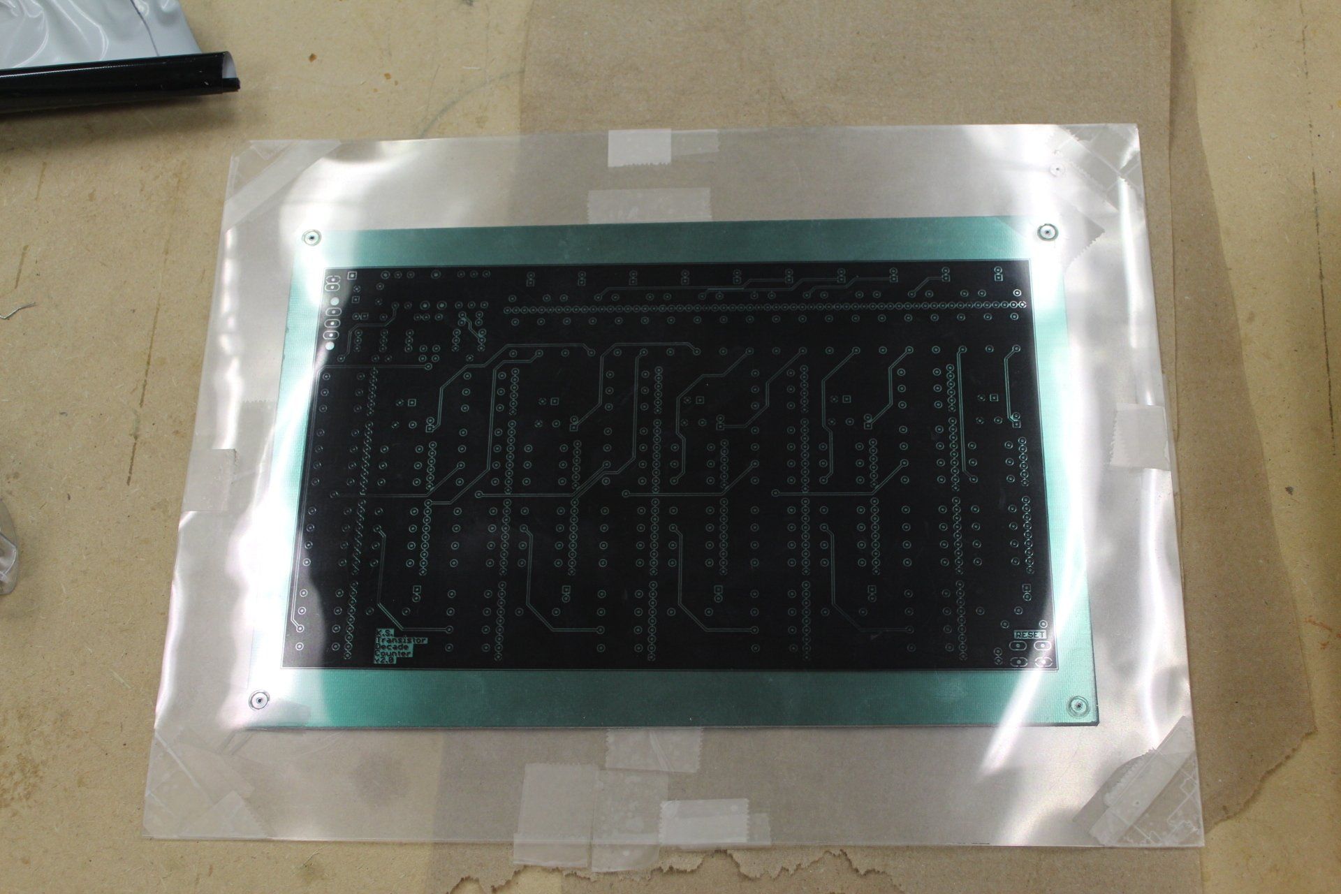
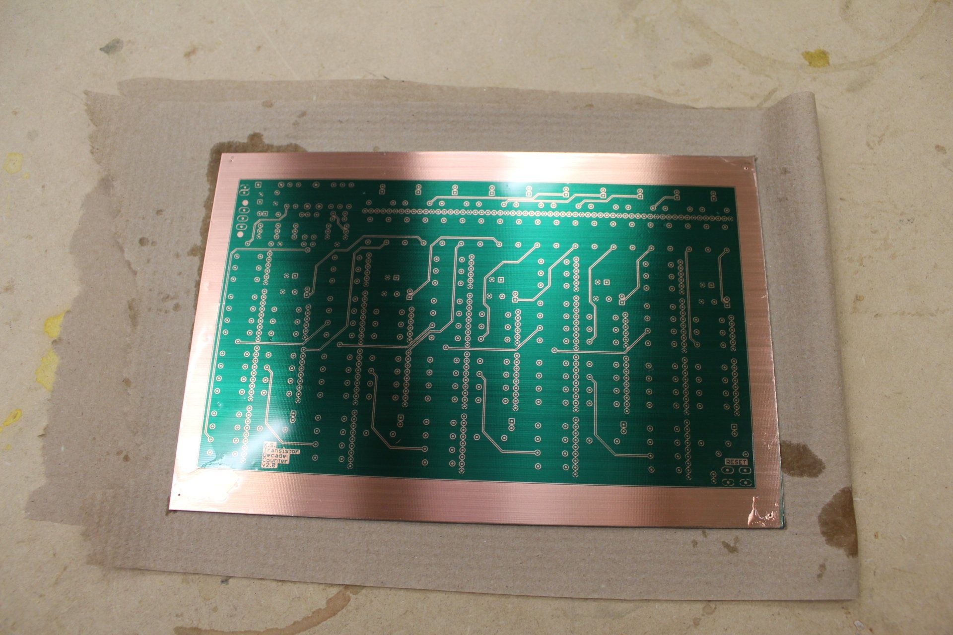
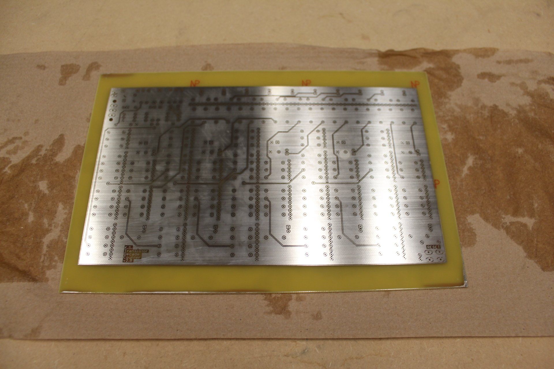
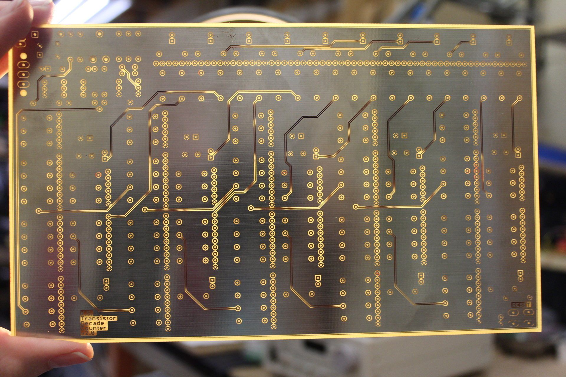
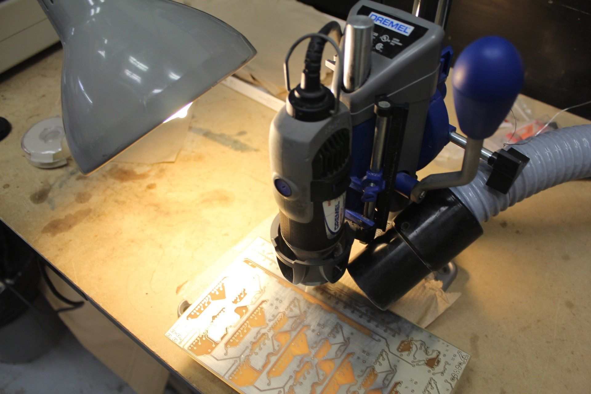
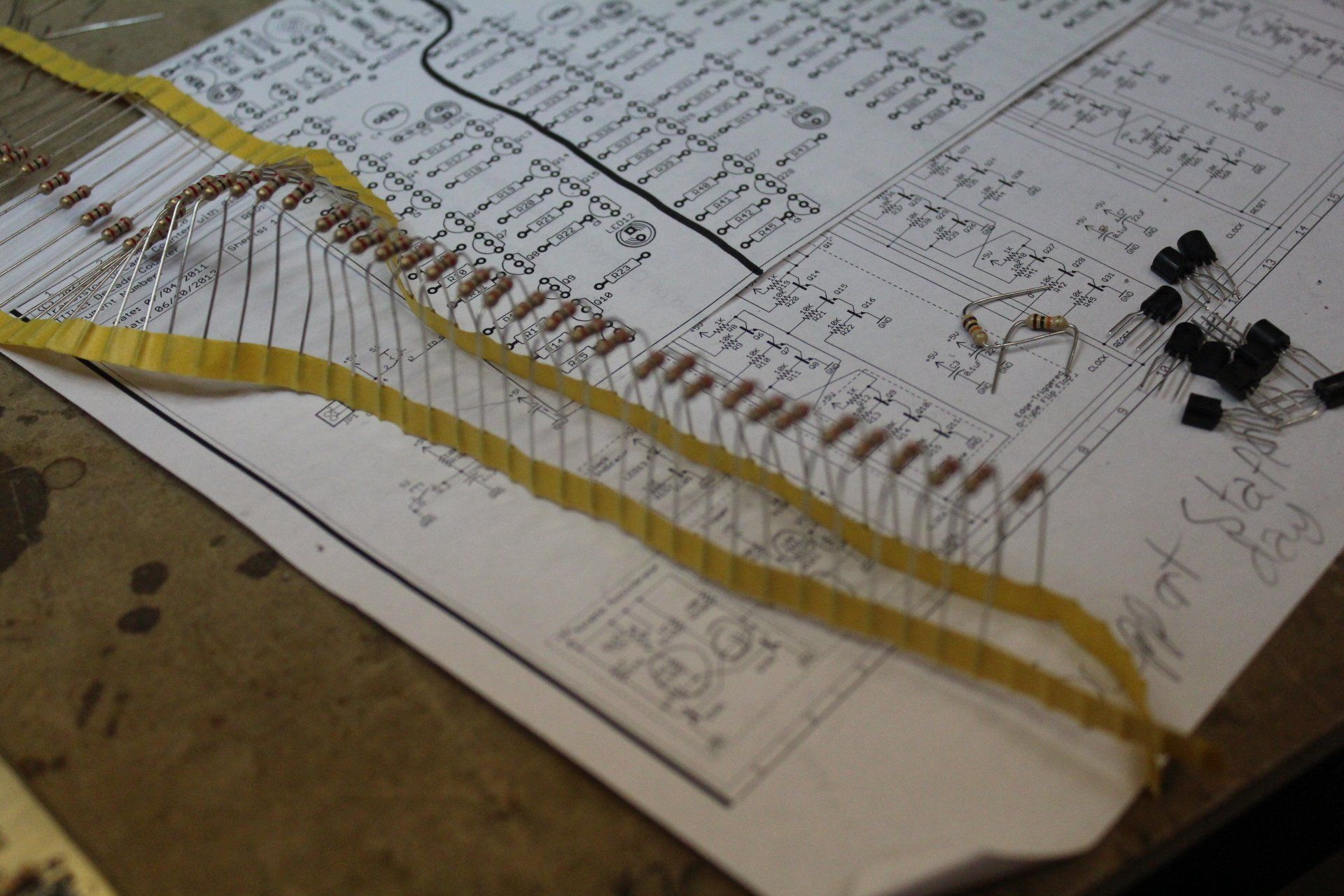
Building the internals of a counter integrated circuit entirely with discrete transistors
This is one of my earlier PCB designs, DIY fabricated as a two-layer PCB without through-hole plating. This circuit is a discrete transistor replica of the classic CD4017 decade counter. Extra LEDs were added to show off the internal logic states of the five D-type resettable flip-flops, and a discrete astable multivibrator provides the clock.
Flow Visualization
Scientific photography is just as much art as it is a means of conveying technical information.
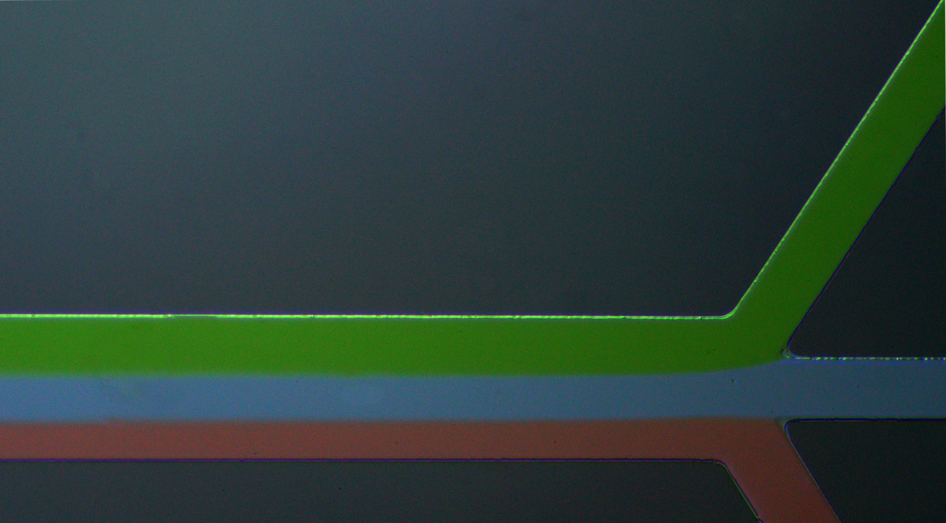
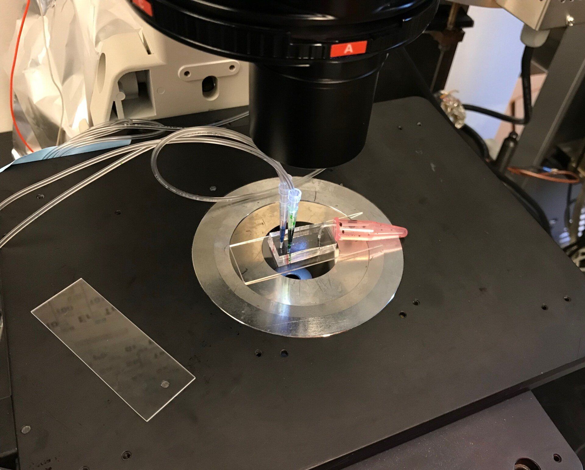
I took a scientific photography course uniquely offered at CU Boulder by Prof. Jean Hertzberg entitled "Flow Visualization". One of my projects made use of the microfluidic channels being manufactured in the Bruns lab by Dr. Hyejin Kwon; fluids behave in counterintuitive ways when forced to travel through channels of very small dimensions. I captured this photo through the optics of an inverted microscope, which demonstrates the lack of mixing between three parallel streams of dyed water in a 400 µm x 23 µm channel.
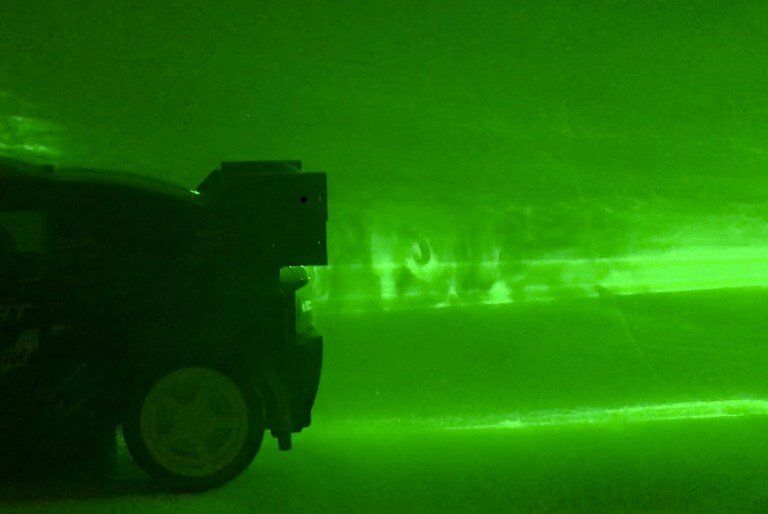
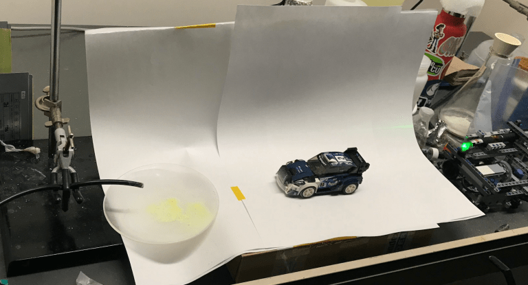
The second image with the LEGO sports car demonstrates a Kármán vortex street; this phenomenon occurs when a laminar flow splits on side of an object but then re-converges on its opposite side. This instability in the flow may cause it to oscillate, generating these characteristic vortices. Normally in air these vortices would be invisible, but can be visualized with an opaque particle tracer. Titanium terachloride spontaneously emits a cloud of white titanium dioxide particles, which are then illuminated with a LEGO-built laser sheet generator (this contraption spins a transparent square LEGO brick at high speed, constantly deflecting/scanning the incident laser beam over a 2-D area).